 Squonk42
At the heart of the FunKey electronic design is the CPU block, built around the Allwinner V3s chip:
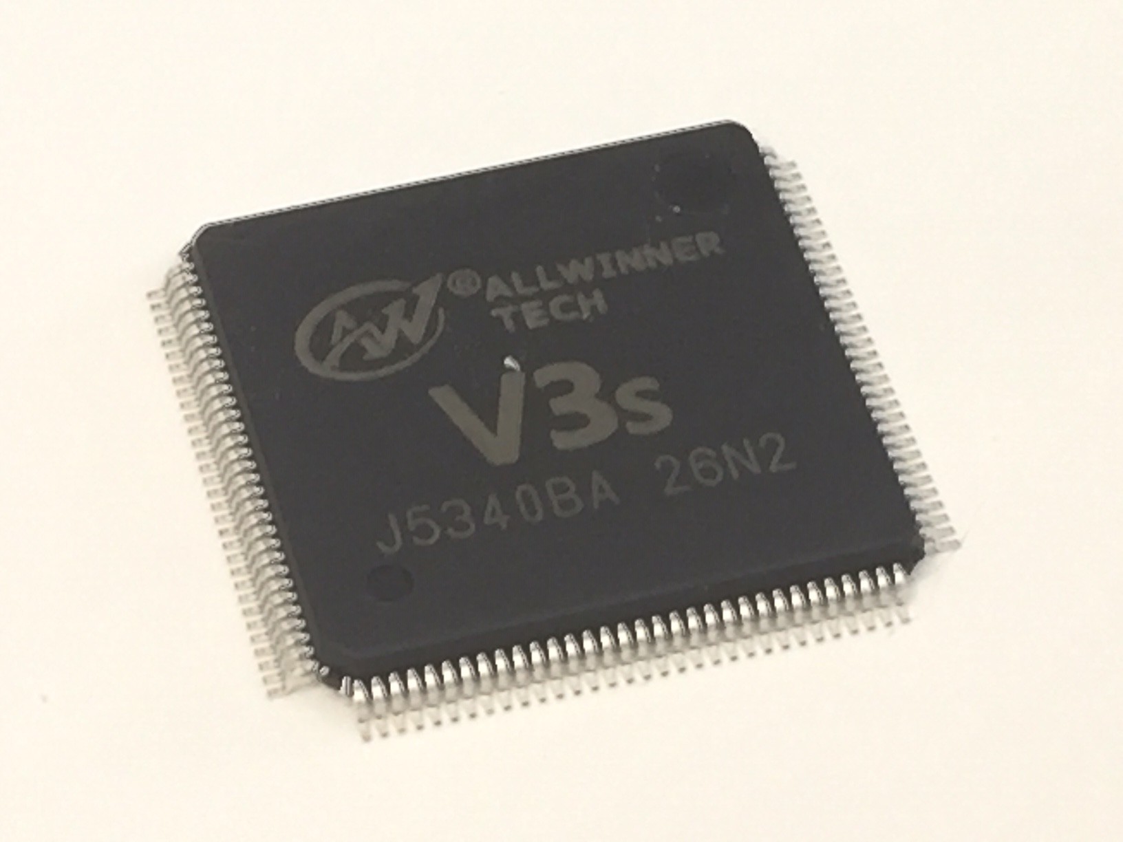
We selected this particular chip because it features a built-in 64MB DDR2 DRAM, which is very good as it saves some precious real-estate on the PCB and also because its layout is much easier: usually because of the mandatory high-speed signals, DDR DRAM requires both length and impedance-matching on all critical signals, leading to the weird "snake"-style layout to balance traces. As here the DDR DRAM is bonded to the CPU into the same package, there is no such requirement here.
OTOH, 64 MB DRAM may not seem much, but we determined that it is sufficient for our modest retro-gaming needs.
One bonus with the V3s is that it comes into a non-BGA (Ball Grid Array) LQFP128 package with actual leads, which is much more user-friendly for prototyping!
Here is the part of the schematics corresponding to the CPU core:

SoC Blocks
As one can see, there is not much besides the CPU chip U3 itself... But it can also bee seen that the CPU is in fact a SoC (System on Chip) containing a collection of built-in peripheral and memory blocks along with the CPU itself:
- the LCD / CSI display peripheral
- the GPIO port G / SDC1 (SD Card #1) interface
- the AUDIO codec
- the LRADC0 (Low-Resolution Analog to Digital Converter)
- the USB OTG controller
- the GPIO port F / SDC0 (SD Card #0) / UART0 interface
- the RTC (Real Time Clock) timer
- the EPHY (Ethernet PHYsical) interface
- the MIPI camera interface
- the built-in 64 MB DDR2 DRAM
- the GPIO port C / SPI interface
- the GPIO port B / UART2 / PWM0 / PWM1 / TWI0 (I2C #0) / TWI1 (I2C #1)
Among these, the FunKey device only uses a few blocks: the AUDIO, USB (as device only), SDC0 (for SD Card), RTC, DRAM, SPI (for the LCD screen), PWM0 (for backlight), TWI0 (for I2C bus to control the GPIO expander and power management chips) and a couple of GPIOs to power the audio power amplifier and get feedback interrupt signals from the the GPIO expander and power management chips.
CPU Power Supplies
What is remarkable though is that the V3s requires a lot of different voltages for its power supply:
- +3V3 for the I/O power supply
- +3V3_AO for the Always-On power supply (RTC timer)
- +3V0 for analog power supply
- +1V8 for the DDR2 DRAM power supply
- +1V25 for the core power supply
This profusion of different power supplies as well as the high power drawn by some of them (1.2A for +3V3, 1.6A for +1.25V) requires a sophisticated power management that will be detailed in a future log.
LRADC0
The LRADC0 (Low-Resolution Analog to Digital Converter #0) is designed to measure the voltage of a resistor ladder switched by keyboard keys: this single input is thus in theory able to manage a keyboard of up to 10 keys @ 250 Hz.
Unfortunately, the FunKey has 12 keys (U/D/L/R, A/B/X/Y, RR/RL, START and SELECT), and the resulting key detection accuracy is not compatible with a gaming usage because of long term stability problems. This is the reason why it is not used in the FunKey and just terminated by a proper low-pass filter R6/C9 to avoid picking up noise glitches.
SD Card
The SD Card interface is almost a direct connection between the chip and the dedicated SD Card connector. Only a single series resistor R8 is required on the clock line in order to prevent ringing.
Crystals
The V3s chips requires 2 crystals: one low-frequency 32.768 kHz crystal Y1 for the RTC clock and one high-frequency 24 MHz crystal Y2 for deriving the 1.2 GHz clock.
The 24 MHz crystal is used by an internal oscillator to lock the phase of the 1.2 GHz oscillator using a PLL (Phase-Locked Loop).
The 32.768 kHz crystal is used by another internal oscillator to tick the RTC (Real-Time Clock) at a standard watch frequency.
These crystals require 2 load capacitors (C12/C13 and C14/C15) each in order to guarantee that the oscillators still start and work with a comfortable operation margin taking into account voltage, temperature and aging.
The 32.768 kHz crystal features an additional high-value resistor R12 in order to limit the internal oscillator's output current and thus reduce further the RTC timer power consumption.
For more details on crystal oscillator design, please check this application note from STM.
DRAM
The DRAM within the V3s chip is a DDR2 one, meaning that its data lines are clocked using both edges of a 400 MHz clock signal.
At these high frequencies, even short wires have a length that is of the same order of magnitude as the signal's wavelength and thus each signal should be considered as a transmission line, for which impedance must be matched to avoid signal reflections, requiring termination resistors on the data lines DQx.
DDR2 or DDR3 DRAMs feature merged drivers and dynamic on-chip termination like this ("VDDQ/2" is labeled "SVREF" in our schematic):
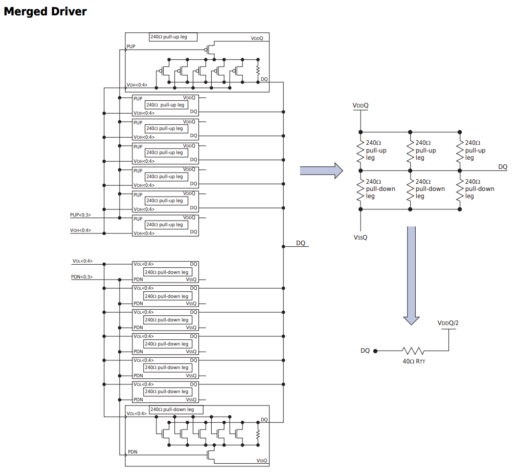
The V3s DDR2 DRAM has an active termination calibration circuitry and procedure called "ZQ Calibration" requiring an accurate 1% 240R resistor R11 (and NOT 240K like shown in the schematic, my mistake!) connected internally like this:
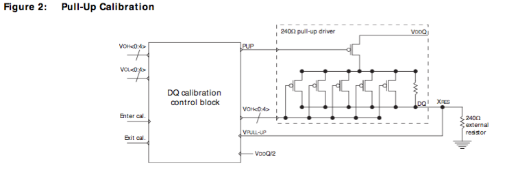
More on the DDR2 DRAM ZQ Calibration subject can be found in this Micron Application Note.
This concludes the study of the FunKey CPU core schematic block.
Discussions
Become a Hackaday.io Member
Create an account to leave a comment. Already have an account? Log In.