 Squonk42
In the FunKey device, the USB interface has 2 purposes:
- provide an external power supply source for both powering the device and charging the built-in LiPo battery
- provide a data interface to transfer firmware upgrades, configuration files, game emulators and game ROMs
The first purpose only requires the +5V USB power and GND pins. The second purpose requires to wire the additional differential data lines D+ and D-. As we only need to operate as an USB device and although the V3s is able to work as either an USB host or USB device using the USB OTG protocol, we don't need the ID pin to determine by the cable wiring which role we must take.
The USB schematic is the following:
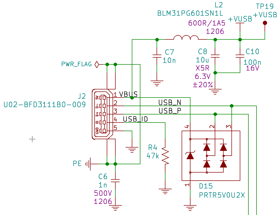
Before connecting 2 devices using an USB cable, they may be at completely different absolute voltages, and during cable insertion, the shield will be in contact before the other pins, including GND. The C6 capacitor between the Protective Earth (Shield) and GND is here to provide an AC path for sinking this difference in voltage and align the GND levels when plugin the cable.
The resistor R4 on the USB ID connector pin should probably not be mounted: as we act only as an USB device, this pin should be left floating.
The capacitors C7, C8, C10 and ferrite bead L2 form a constant-k 3 pole CLC low pass filter to remove any spurious in/out on the USB power supply wire. The USB 2.0 specification limits the maximum bulk capacitance value to 10 µF in order to avoid power supply excessive droops when plugin in a device with a discharged large bulk capacitor.
D15 is a combined TVS protection diode for the VBUS pin and a set of clamping diodes that will limit the voltage on D+ and D- pins to stay between GND and VBUS levels to in order to protect the V3s USB driver from under / over-voltages.
Discussions
Become a Hackaday.io Member
Create an account to leave a comment. Already have an account? Log In.