 CapitanVeshdoki
Today I partly redesigned schematics of control circuit and traced beta-version of PCB.
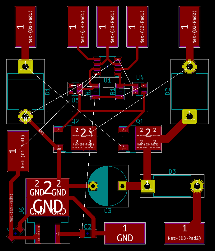
Now it looks like this:
Realized, what "forbidden input state" for Set-Reset latch (two NORs near bottom-right corner) leads only to uncertainty and fatal for simulations only. So! I just threw out AND and NAND gates, as they simply messed my PCB without a large practical sense. Schematics looks much more convenient without them :)
Also I connected V1_REF, I_COIL and V2_REF inputs more precise.
It looks simple, but hey! So much things to control here:
- Energy of an impulse (through V1_REF and V2_REF)
- Lowest voltage of impulse (V_TRG, target voltage) aka impulse duration, since with bigger voltage you can achieve bigger currents, faster energy dissipation. Voltage on capacitor C3 should be greater (due to charge during demagnetization) or equal to V_TRG
Here is how PCB probably would look like:
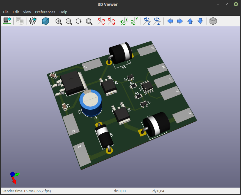 P.S. Capacitor is going to be external in this version, to find needed capacity
Main question for now - how to produce it. I'm not into making two-layer PCBs at home (too impatient for it, even if process is encouraging), I would try to trace everything on one layer with minimum wiring.
Discussions
Become a Hackaday.io Member
Create an account to leave a comment. Already have an account? Log In.