After long study nights and exhausting exam sessions, I finally found some time to get started on the attempt to design the PCB from scratch.
The original PCB from Bang & Olufsen is a beautiful single layer board with no SMD parts whatsoever.
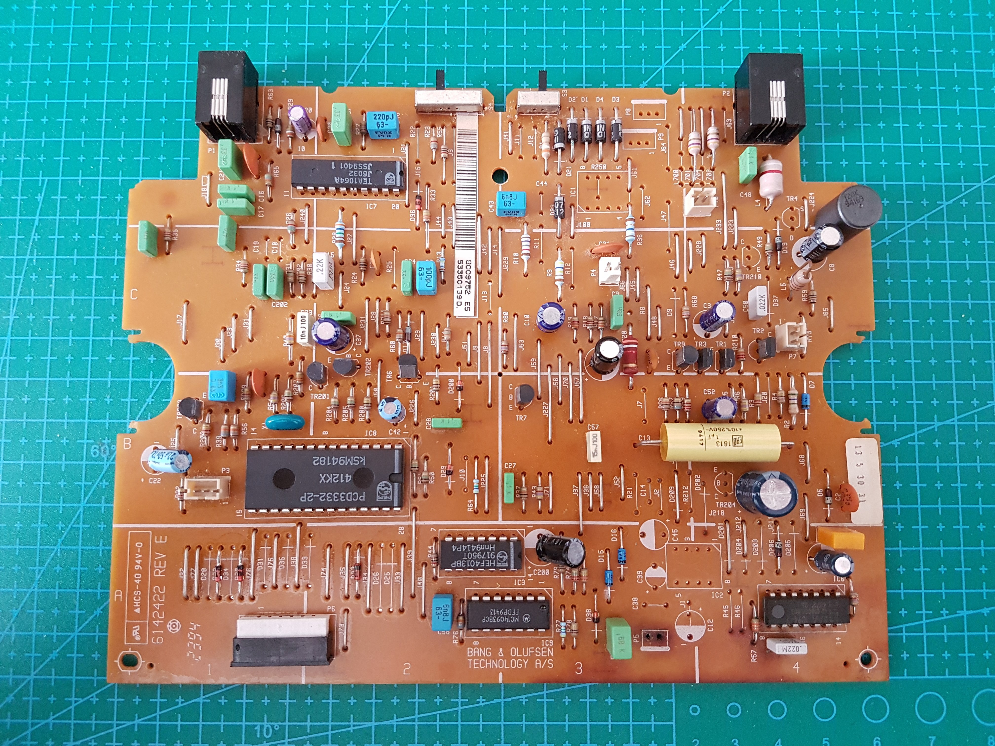
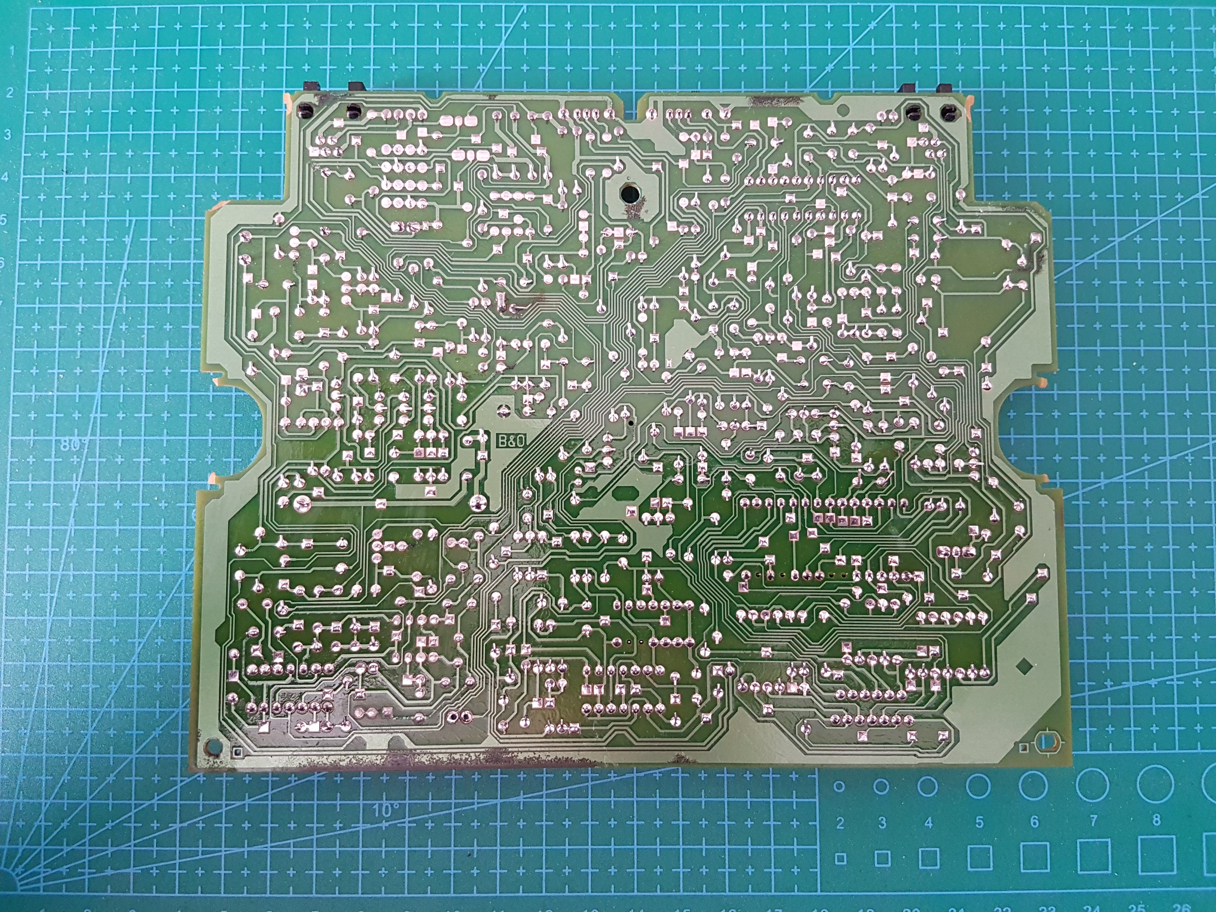
My board is not working, and on top of that, the backup AA battery went off a long time ago, and as a result, the bottom part of the PCB is corroded as well.
As you can see, there are two switches on the top. On a sticker on the bottom of the phone, the right one has 3 states, labeld from two to zero, and the right one has two states: IWV and MFW
Needless to say, I have no idea what those switches do.
After measuring the board in all of its dimensions, I then recreated the board geometry on EasyEDA.
The board interfaces to the various component of the phones through connectors, which I think require two B2B-ZR sockets for the two microswitches that open and close the call, one B3B-ZR socket for the volume potentiometer and a Molex KK style socket for the loudspeaker.
Here's the mockup:
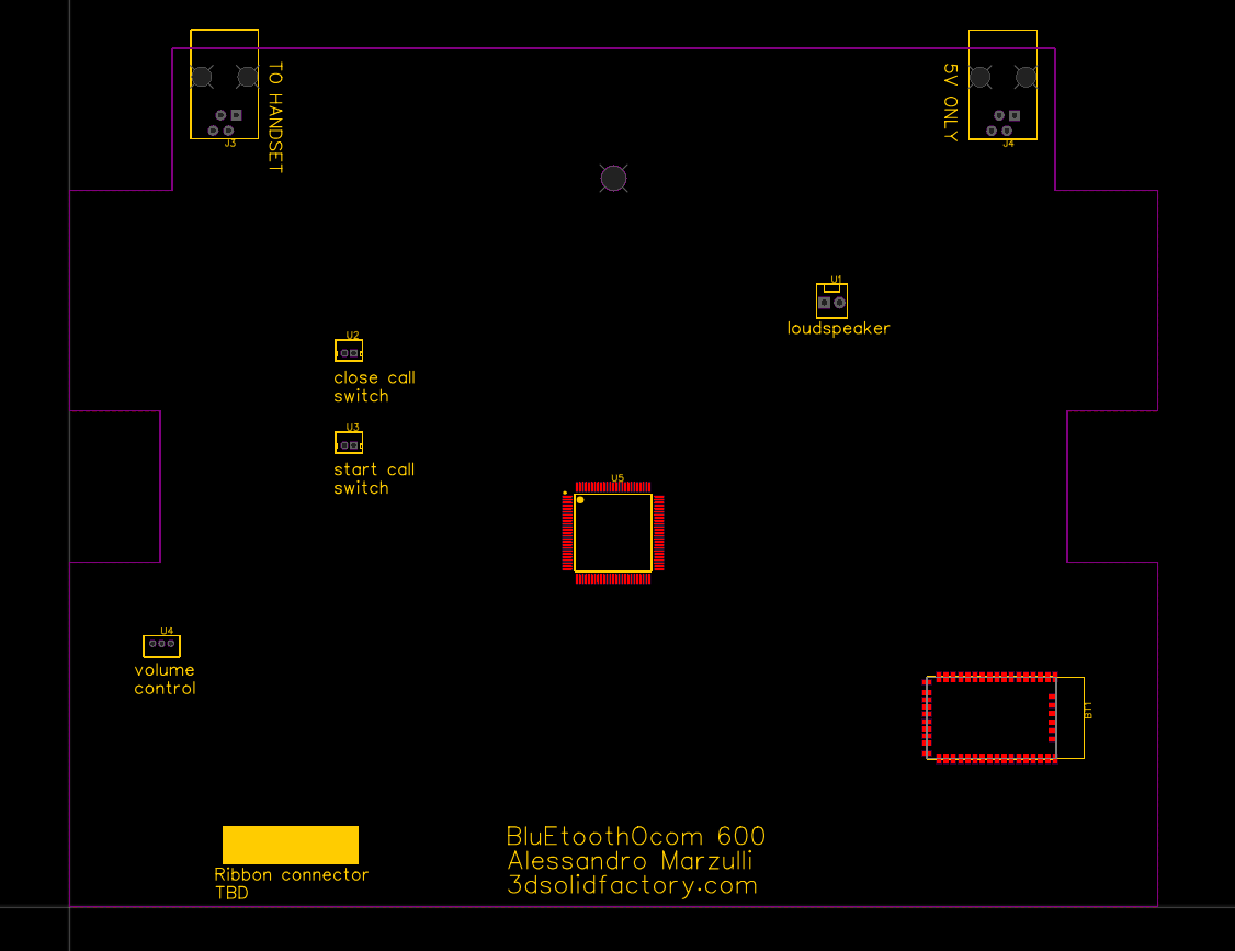
The MCU can be then programmed to use both of those switches to start and end a phone call.
Here's a picture, so you can see the white lever pushing on only one swith at a time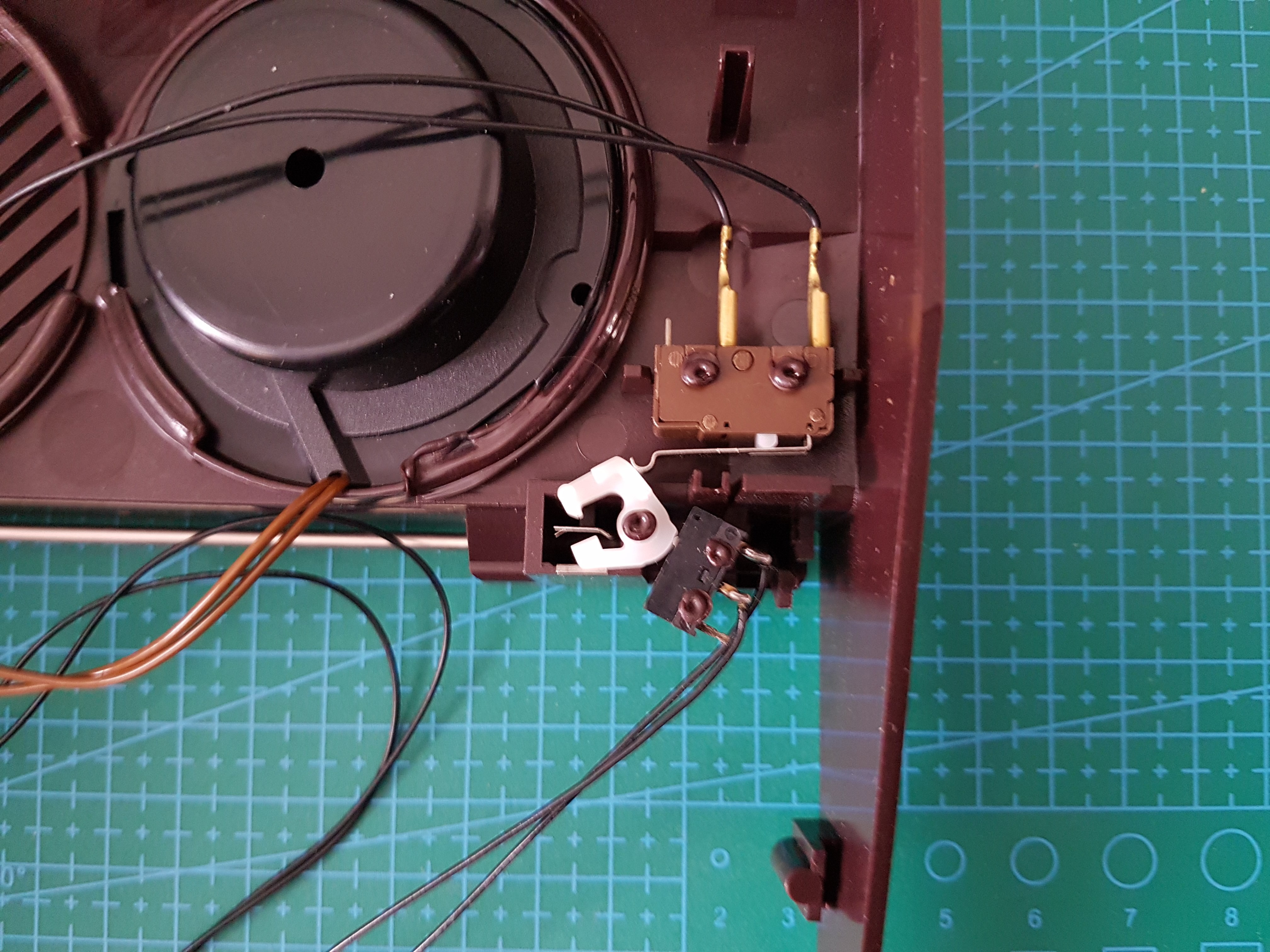 (As you can see, almost everything is welded to the chassis itself, rendering any attempt of further teardown destructive.)
The only big problem though, is the keypad ribbon connector.
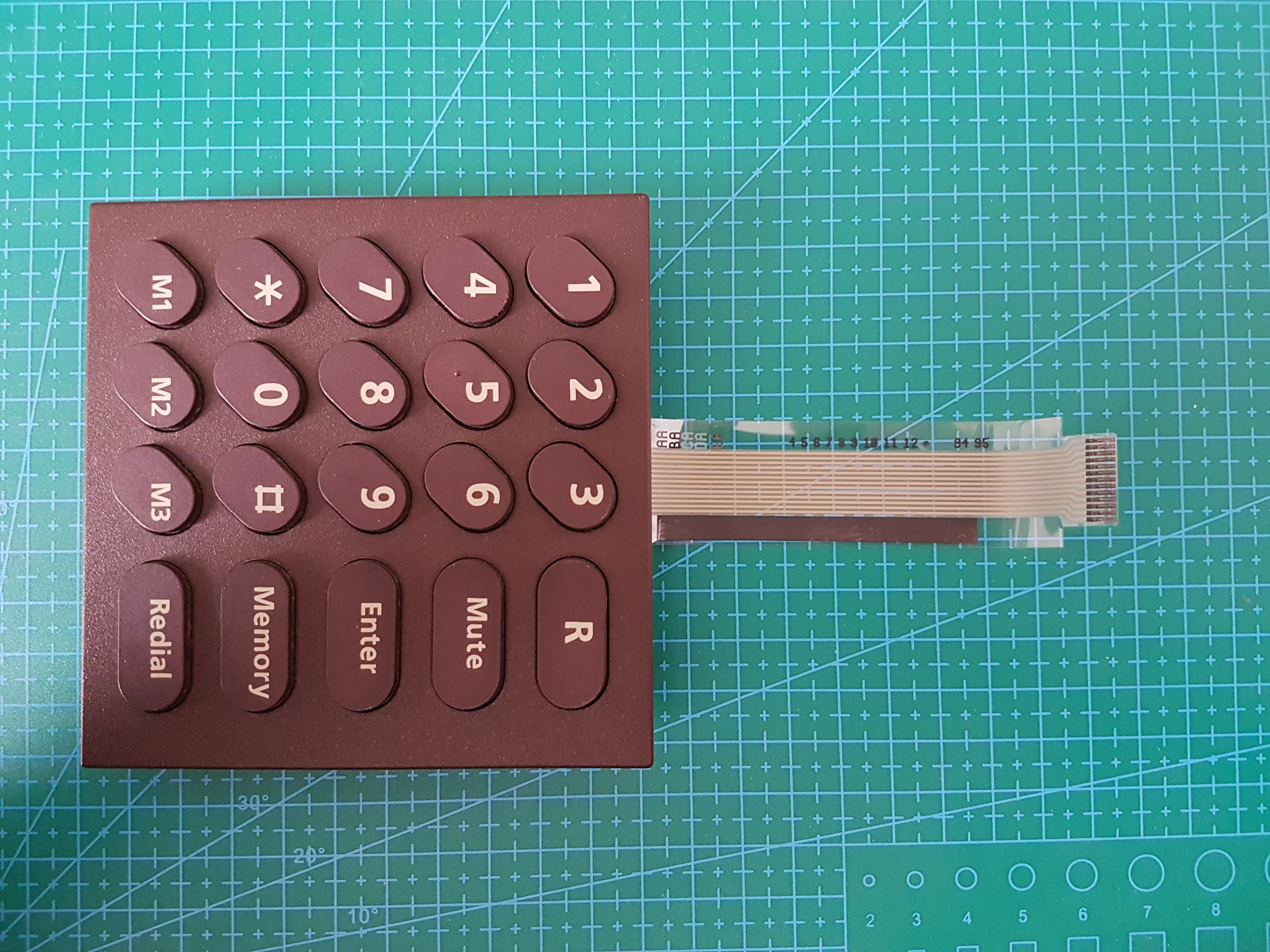 The keypad is a 5x4 matrix, but it has a 13 pin connector. Probably some pins are not connected, but reverse engineering of the keypad will be the next step.
Right now, i'm having issues to find the proper socket.
You can just desolder the one on the original PCB and call it a day, but the aim of this project is to make a replacement PCB that won't require any component transplant From the original B&O PCB.
As usual, if you have any suggestion either for a suitable and cheaper bluetooth module or for the flat cable stocket, fell free to leave a comment on the discussion section
Discussions
Become a Hackaday.io Member
Create an account to leave a comment. Already have an account? Log In.