 Lucy Fauth
To overcome these issues, GaN and SiC switches require some special gate drivers (eg. with a output voltage of -6 to 10V. The negative voltage helps to bias the gate against mentioned voltage spikes during turn-off.) located as close as possible to the switch.
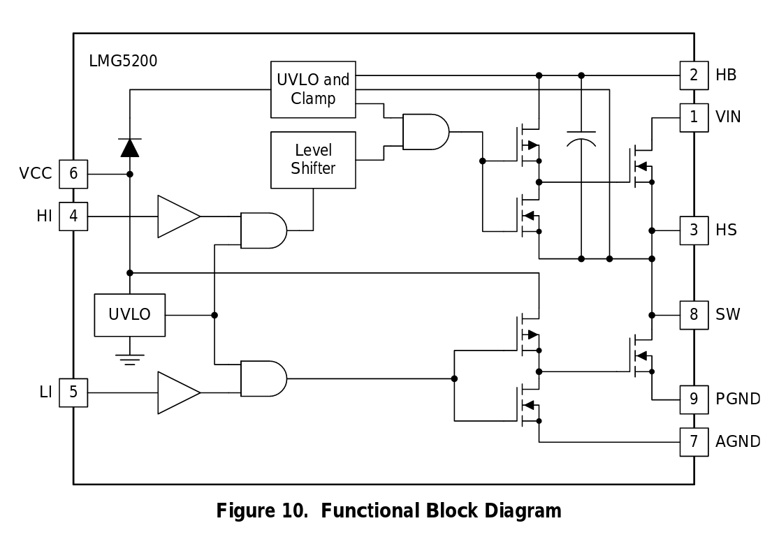
(http://www.ti.com/lit/ds/symlink/lmg5200.pdf)
The latest schematics of the full design can be found here: https://github.com/NiklasFauth/pcbtc/blob/master/hardware/schematic_V1.5/pcbtc.pdf
We can separate the design in five functional blocks:
- STM32 microcontroller
- Flyback boost converter
- Feedback signal recovery
- Deadtime circuit
- GaN full bridge
Revisions
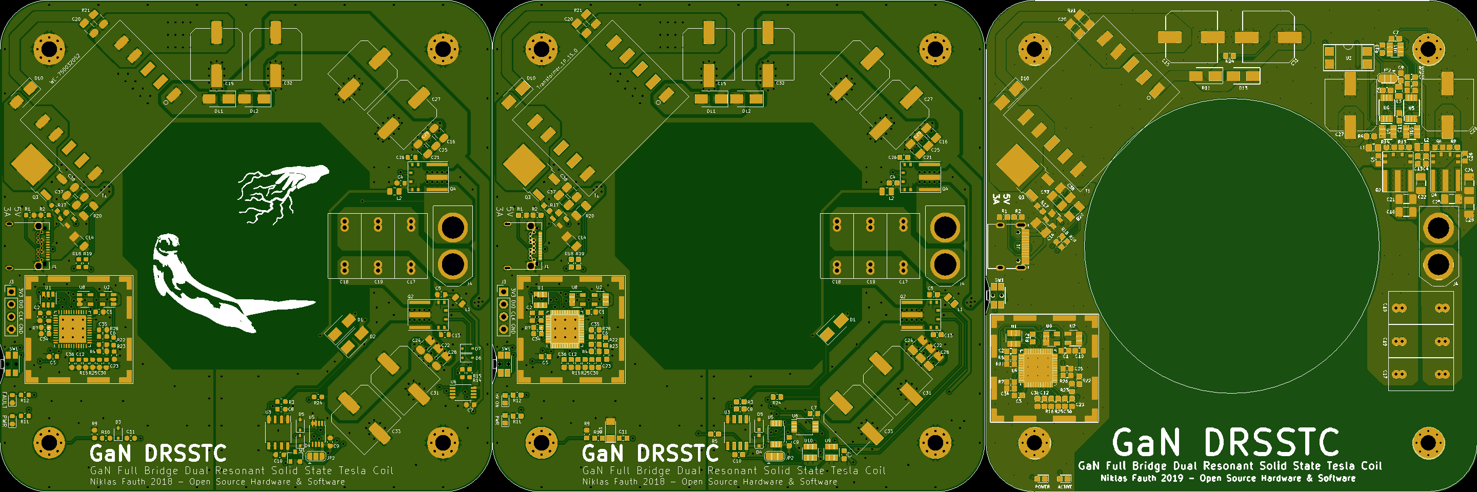
(three selected design revisions. From left to right: V1.0, 2018-11-22 - no dead time, bad power layout; V1.3, 2018.12.22 - dead time, first arcs, GaNs randomly die after 1-20min; V1.5, 2019-12-04 - good performance, good reliability - still room for optimization ;)
In total, it took 6 pcb and design revisions to get the current performance and reliability. This is mostly due to the very challenging requirements that come with the use of GaN switches. Some pcb revision could have been avoided if I would have followed the recommendations in the datasheet in the first place. Usually, you can interpret design guidelines and maximum ratings as "recommendations" - this is definitely not the case when it comes to GaN and SiC design. When TI writes about placing components "as close as possible" like they do on page 10, 13, 14, 15 and 16 of the datasheet - 8 times in total! - they really, really mean it like that. "Close" does not mean "nearby". "Close" does not mean "right next to it". "Close", in terms of low parasitic inductance, means: on the opposite of the board, right under the according pads, connected with as many vias as you can stick in there.
I had to learn this the hard way - I might have killed 10 LMG5200 modules because I though I knew better. But more about layout considerations, later. Let's start with the easy stuff:
STM32 microcontroller
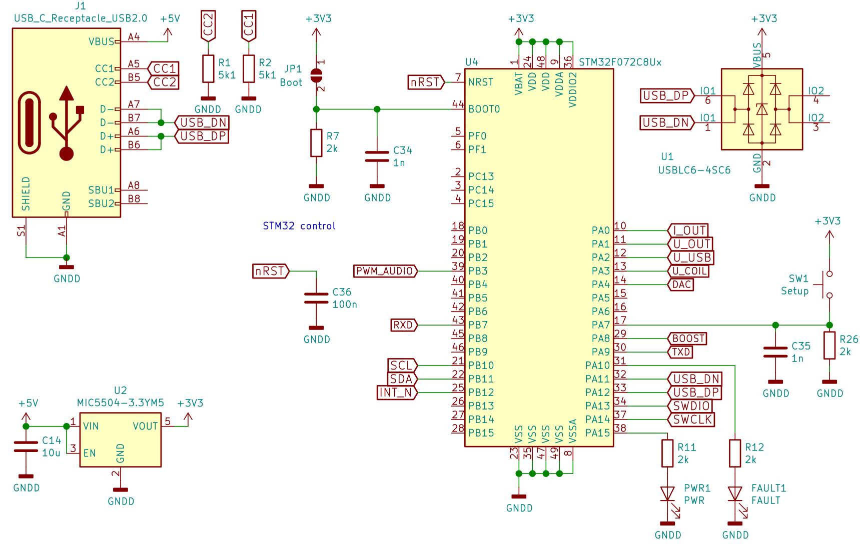
(yes, it looks like USB DN and DP are shorted - the schematic symbol is for a USBLC6-2SC6, but I'm using a USBLC6-4SC6. I'll fix this soon but no worries, it's just graphical)
There is nothing too special about this. I used the STM32F072 for this project, one of my favorite parts from the STM32 series. The STM32F072 is cheap, has a proper ARM M0 core, and supports crystalless USB operation by using clock recovery / syncing from the USB frames. So you get a decent Micro with USB and lot's of STMs powerful timer peripherals for under $1 that requires minimal external components. I used the QFN version because I find it much easier to solder than QFP.
Also, the STM32F072 has a DFU bootloader - this means you don't need any programer to flash the firmware. For the initial flashing, you have to temporally bridge a solder jumper on the back of the pcb - the tesla coil will now enumerate as a DFU bootloader device and you can flash the firmware eg. with dfu-util. Once flashed, you can press the button on the pcb to jump into the bootloader to update the firmware.
Discussions
Become a Hackaday.io Member
Create an account to leave a comment. Already have an account? Log In.