 Lucy Fauth
Flyback boost converter
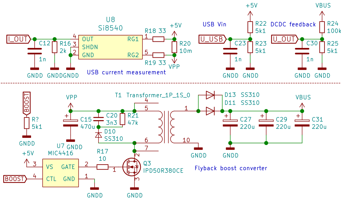 The flyback
converter steps up the 5V input voltage to 40-50V for the GaN
full-bridge. As the turn ratio of the tesla coil already is at a max
(you can’t have less than one primary winding ;) the only way to
get higher output voltages is a higher input voltage. A flyback
converter doesn’t work like a traditional transformer, it it much
more comparable to a boost converter: The transformer acts as a
coupled inductor that stores magnetic energy in the air gap.
Independently of the turn ratio, output voltage can reach
(theoretically) indefinitely high output voltages. The only
difference is that with a well-chosen turn ratio, efficiency can be
improved a lot compared to a simply boost topology.
The flyback
converter steps up the 5V input voltage to 40-50V for the GaN
full-bridge. As the turn ratio of the tesla coil already is at a max
(you can’t have less than one primary winding ;) the only way to
get higher output voltages is a higher input voltage. A flyback
converter doesn’t work like a traditional transformer, it it much
more comparable to a boost converter: The transformer acts as a
coupled inductor that stores magnetic energy in the air gap.
Independently of the turn ratio, output voltage can reach
(theoretically) indefinitely high output voltages. The only
difference is that with a well-chosen turn ratio, efficiency can be
improved a lot compared to a simply boost topology. The PWM for the
switching mosfet is generated by the STM32. The STM32 thous has full
control of the output voltage, allowing things like slowly ramping up
output voltage to not overload USB, software-configurable bridge
voltage and potentially QCW-DRSSTC operation.
Deadtime circuit
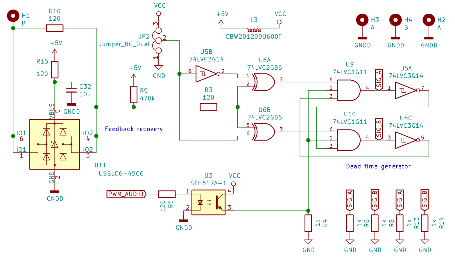
The so-called shoot-through condition happens when both switches in a half-bridge design are conducting simultaneously. This usually doesn’t happen intentionally, it rather happens as a side effect during switching: If you switch on one fet in the exact same moment you switch off the other, due to time delay mismatch it can happen that for a very short period of time, both switches are conducting, usually causing death to both fets. To counteract this unfortunate event, you can add a small amount of time where both fets are off, “break before make”, or, in EE slang, dead-time.
Even though the LMG5200 already integrate an impressive amount of circuitry, one thing missing is dead-time logic. Texas Instruments arguments that this is an advantage as it gives the designer the freedom of controlling the two individual GaN devices in the half-bridge as they wish. However, it also gives you the freedom to kill both GaN Fets if you turn them on simultaneously.
I didn’t realize that in my first attempt, and adding dead-time logic was the milestone that lead to the very first sparks from this design. The circuit is pretty easy: Two triple-input AND gates are feed with the feedback signal, one inverted, the other not. Also, enable from the STM32 is applied to both AND gates. The opto-coupler was added to separate the STM32 from the electronics for the tesla coil: As you will learn later, the GND for everything related to driving the LMG5200 is on a separate ground plane, only conneted to power ground through the LMG5200 itself. This is again because the fast switching of the LMG5200 can induce voltage spikes that can lead to unwanted behavior. The opto-coupler is there to connect these to domains without introducing noise to this separated ground plane.
The third input is the inverted output of each other AND gate: Only one of them can output high at a time, as they are blocking each other. As the signal has to pass through the inverter first to enable the output of the other AND gate, the delay time of the inverting gate is added to the signal as dead-time where both AND gates outputs are low.
Feedback Signal recovery
Is is very important for the tesla coil to operate at it’s own resonant frequency. However, this is not a fix value, it heavily changes during operation: Both the amount of metal in the surrending as well as the very arc created by the tesla coil forms an additional capacitance that decreases the resonance frequency. The easiest way to follow these changes is to operate the coil in a self-resonanting mode: The output of the coil is sensed, amplified and feed back to the driving circuit as positive feedback. This causes an undamped oscillation at the resonant frequency.
There are multiple known attempts to recover this feedback signal. The biggest difference is either it is recovered from the primary resonance circuit or the secondary coil. The easiest way is to sense the current flowing through the secundary coil using a shunt resistor in series with the earth connection. This is the method as seen in the schematic above, however, it implicitly couples RF noise from the discharge into the logic circuit, which might cause the problems experienced when touching the discharges.
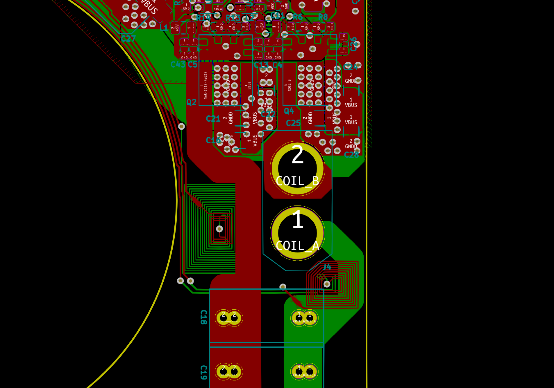
Another attempt is
to sense the primary current and use this signal to drive the GaNs.
This methode is usually more robust and can be used and tested even
completely without any secundary coil. Traditionally, ~1:100 current
transformers wound to a small ferrite torus core have been used for
this. For my coil, this is too big, and also I didn’t wanted to add
additional inductance in the primary resonance circuit as even the
short wire going through such a ferrite would add a higher inductance
than my whole primary coil. Instead, I used the advantage of my high
frequency design, and tried using a air-coupled current transformer.
This design will be evaluated within the next few weeks.
Discussions
Become a Hackaday.io Member
Create an account to leave a comment. Already have an account? Log In.