 Bud Bennett
I need the heater to keep the reference PCB at a constant temperature while the ambient temperature varies from about 10°C to 30°C. The heater PCB will be about the same dimensions as the reference PCB in order to fit into the case. I expect to insulate the two boards with about 1/2" of open cell foam, with a thin piece of foam separating the two boards within the enclosure.
To wit, I set about to determine how much power the heater would require to keep the temperature at the desired value. There is a lot of fat finger estimation going on here, but you gotta start somewhere. If I get it wrong it's not the end of the world.
I found that the amount of power needed to drive the system to 30°C from about 18°C is surprisingly small -- only about 2W, depending upon the degree of insulation within the box.
The Experiment:
I have a couple of PCBs that are populated with an array of 10Ω/1W carbon resistors that were created explicitly to be a heater. I enclosed one of these PCBs in a sandwich of open cell foam with a thickness of about 1/2 inch. I made a good effort to seal the edges to prevent air movement and leakage. I also placed a K-type thermocouple lead in the middle of the PCB to take the necessary temperature readings.
The experiment consisted of applying a known power dissipation across the PCB and measuring the temperature rise from ambient temperature after the internal temperature was allowed to stabilize. The purpose of the experiment was to estimate how much power would be necessary to keep the temperature internal to the enclosure constant over the expected external ambient temperature range.
The Results:
I applied exactly 1.0W of power to the resistor array and waited until the temperature stabilized -- about 1 hour. The difference between the internal temperature and the ambient temperature was 11°C. I then applied 2W of power and got a 22°C rise. I measured a 33°C rise with 3W applied. This translates to a thermal resistance of 11°C/W.
I also ran a simulation of the proposed heater circuit to see how the power dissipation varied between the active devices and the passive devices. The green trace is the power dissipation in the FET (or voltage source in the simulation), the blue trace is the power dissipation across the resistors, and the red trace is the total power dissipation in the circuit. It turns out (no surprise) that the preferred power dissipation should be between Pmax and Pmax/2 so that the passive devices dissipate most of the energy instead of the active device. Here's a plot of the relative power dissipation between the FET and the resistors. I was assuming that the heater would require 10W maximum which was too high by a factor of three.
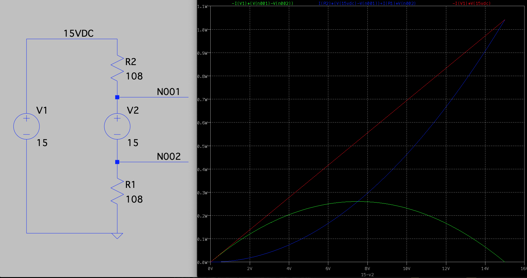
But it is interesting to note that the maximum power dissipation of the active device peaks when there is 1/2 the supply voltage across it.
The Design:
This is the first pass of the design for the heater:
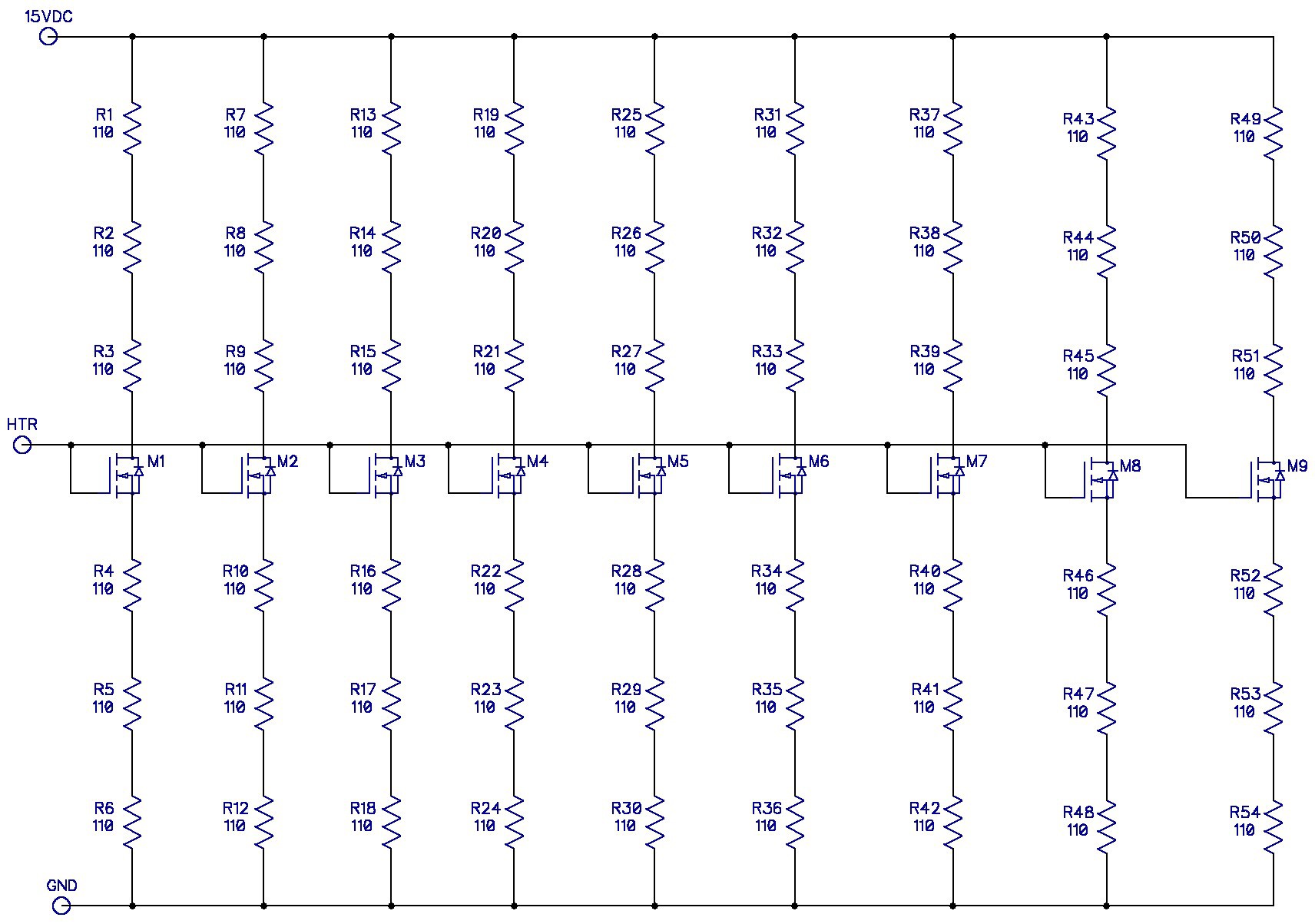
When there is nearly zero volts across the AO3400 FETs the maximum power dissipation is a bit over 3W: 9 x 15V^2/(6 x 110Ω). In that case the power will be dissipated across all of the resistors and very little power consumed by the FETs.
The smallest estimated power dissipation is about 1W, when the ambient temperature is 80°F (27°C) and the circuit is attempting to keep its target temperature at 100°F (38°C). In this case most of the power is dissipated across the FETs, but it is not a significant amount and the expected temperature rise is only about 6-8°C in the FETs. I estimate this based upon the AO3400 data sheet which claims that the thermal resistance from junction to ambient is between 80-100°C/W.
The resistors are 2512 smd 5% tolerance. They are rated at 1W maximum dissipation/each, with an expected thermal resistance of 80°C/W.
If I get it wrong, then it is a simple matter to order resistors with a difference value to populate another Heater PCB. Here's what the PCB layout looks like today:
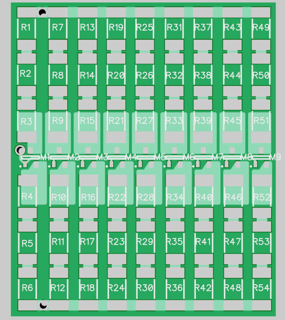
I placed a lot of metal around the FETs to distribute their heat across the PCB. There is also a large ground plane on the back side (which will face the refrerence PCB) to help even out temperature differences even further. The PCB is the same size as the reference PCB to make the packaging easier.
Discussions
Become a Hackaday.io Member
Create an account to leave a comment. Already have an account? Log In.