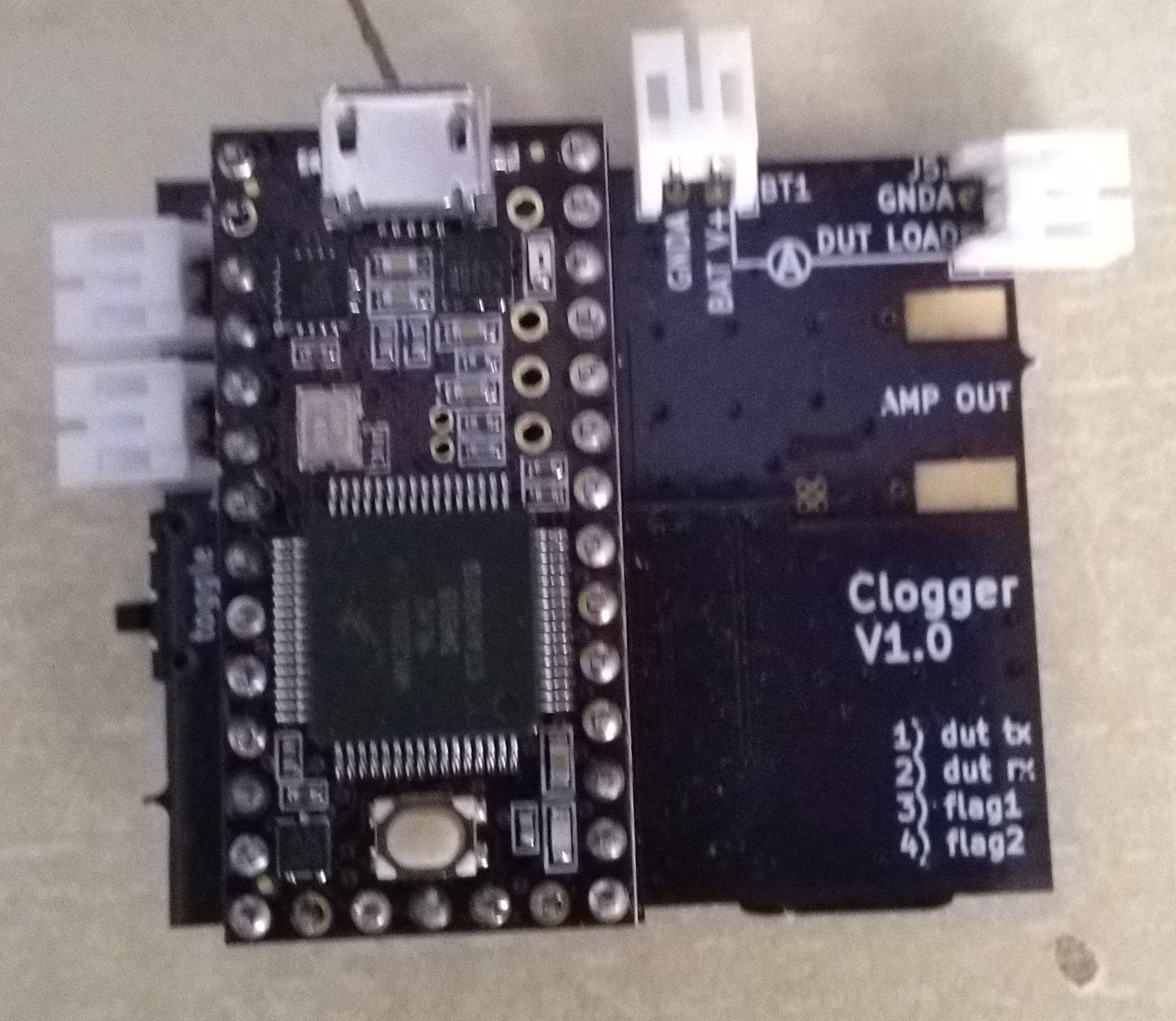
• Now with 90% more reality!

    justinbrowe07/02/2019 at 12:08 1 comment

    Thought has become action and action has given way to existence. That which once was not now is.

    I have assembled the first Clogger board. 

    In the process, I noticed that I forgot to put decoupling caps on the fancy 24 bit ADC, so we will see if it even works - I might have to do the first board rev just to fix that.

    I can't really test it until I have drivers for the ADC, so I am working on drivers for the ADC now.

  • Schematic and board

    justinbrowe05/29/2019 at 23:59 0 comments

    I decided to follow the suggestion by K.C. Lee to use a current sense amplifier, but to add a dummy load to push it into the linear region.

    The advantage to using the current sense amplifier is that the clogger will work for a wider range of supply voltages (for the device under test). The max4428f is also less expensive than most of the instrumentation amplifiers that I was looking at.

    For the dummy load, I just used a current mirror.  I am not sure how stable the load will be across temperatures, but the best way to find out will be to build the thing and test it.

    The power supply for the device under test is reverse voltage protected. The Teensy 3.2 has 5v tolerant pins, so I decided not to level shift the uart and flag signals.

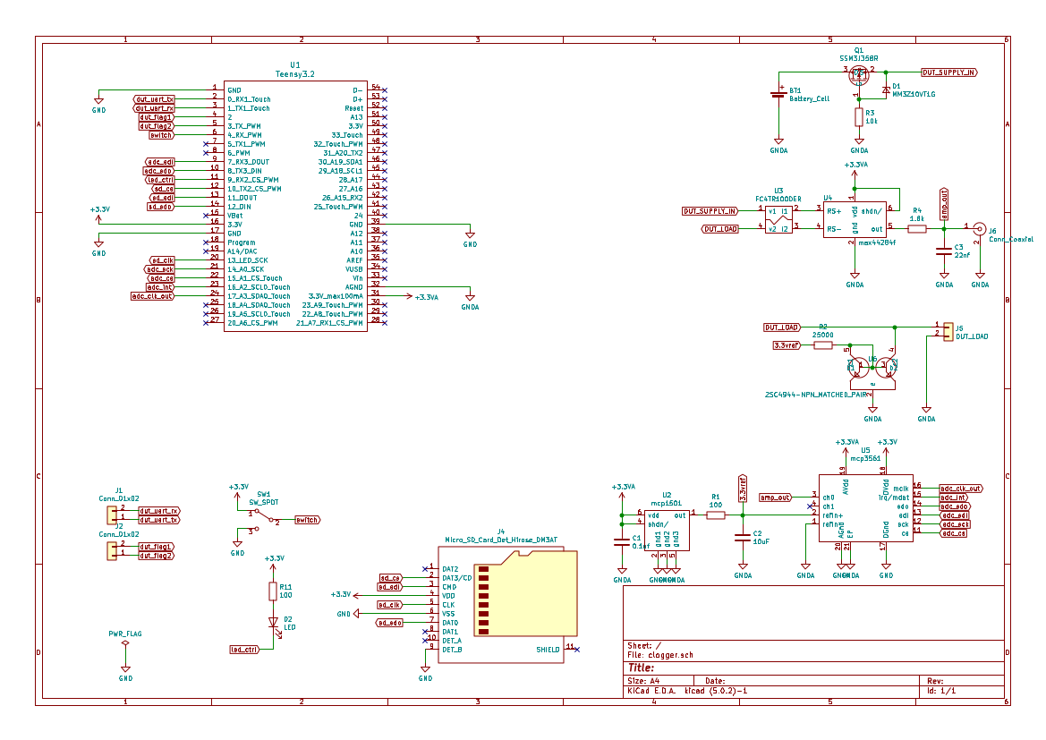
    I wasn't completely sure about the best way to ground the system. The Teensy 3.2 exposes an analog ground pin that I think is connected to the main ground through a choke, so I grounded all of the analog components through that one ground point. However, I wasn't sure how to ground the the device under test. Most of the devices that I hook up to the Clogger will have high speed clocks and dynamically changing loads ... but that exactly what I am trying to measure. I decided to ground the device under test to the analog ground.

  • Amplifier take 2ish

    justinbrowe05/07/2019 at 22:43 1 comment

    K.C. Lee referred me to the MAX44284, which was helpful. Its specs were close to those of the MAX9923F that I was looking at, but it smaller and almost half the price at scale!


    v offseti bias
    gain error
    CMRRVo min
    $pk
    MAX4428420.5uV80nA0.15%145db1mV-20mV
    1.19
    MAX9923F10uV1pA.5%140db10mV2.1

    Maxim also offers a spice model of the MAX44284f on their website, so I set up a simulation just to confirm the problem I noticed the other day.

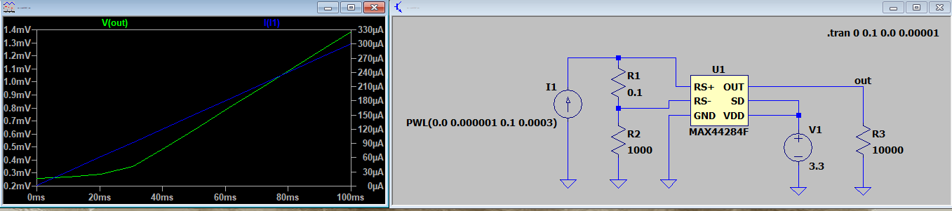
    The amplifier doesn't start to behave until the supply current reaches ~40uA. which is pretty far outside my spec.

    Instead of using a current sense amplifier, I am going to use a instrumentation amplifier - probably the max4209.

    Instrumentation amplifiers are not cool with common mode voltages outside their supply voltage range, so this design will prevent people from power-debugging devices with supply voltages > 5v, but I think that is acceptable. This is a tool for optimizing the battery life of low-power devices and most power-sensitive battery operated devices are going to have supply voltages <5v.

    I had to use the reference pin to add in a 0.2v offset voltage. This is going to take a small bite out of my ADC range, but the ADC I am using has some programmable amplification options that will allow me to counteract that loss a bit. I think I am going to move forward with this design.

  • Un-picking the amplifier

    justinbrowe05/04/2019 at 23:59 2 comments

    The purpose of learning is to expose the lies we have accepted in our model of the universe. To pursue truth is to feel more acutely its absence. If anyone would learn, they must remember what they have 0.00005forgotten that they did not know.

    Deep.

    The MAX9923 is not going to work. Actually, none of the amplifiers that I picked are going to work. While looking for a spice model of the MAX9923 I came across a good article by maxim about estimating error sources for current sense amplifiers.

    They identified five different sources of error, explained what they mean and how to calculate them, and linked to a useful online calculator. As I expected, a large portion of my error came from the offset voltage of the amplfier, but the error due to the common mode rejection ratio was actually way higher (228uV vs a conservative 50uV on the output side).

    The common mode rejection ratio described the ability of the amplifier to reject variation on the input signals that is common to both. They way that they say to estimate the error from this term is to compare the common mode voltage that you expect your system to use to the common mode voltage at which it was characterized. The datasheet says that tthe MAX9923 was characterized at a common mode voltage of 12V, and I am expecting use voltages between 4.2V and 2.9V. According the maxim article, unless I use common mode voltages close to 12V, I am going to get errors that completely drown out my signal. Even though the datasheet says that common mode voltages can range from 1.9V to 28V, the further the common mode voltage is from the voltage it was optimized for, the larger the effects of the common mode rejection error are going to be. None of the amplifiers I looked at were optimized for the range in which I want to work.

    On top of that, the error calculator revealed to me that the MAX9923 has a specified output range. According to the datasheet, the min output voltage is between 1mV(typical) and 10mV(max). Using the highest gain amplifier, I would have to use a sense resistor of ~8Ohms to product satisfactory output voltages at my minimum current spec of 5uA. At my max current spec of 100mA, this would mean a voltage drop of 0.8V - way too much.

    What does this mean? 1) common mode voltages are going to make it very hard to measure small currents. 2) I am either going to need higher gains or an amplifier with a lower minimum output voltage.

    Practically, I think this means that I have to give up on using a high-side measurement system. A low side system will get rid of the common mode voltage problem and will open up more amplifier options to me.

  • Picking the ADC and microcontroller

    justinbrowe05/04/2019 at 02:14 1 comment

    After digging through the bowels of digikey, I have picked the microchip MCP3561 for the analog to digital converter. It is a 24 ADC with a maximum sampling rate of 153.6kHz and can talk over SPI at 2MHz. It can also perform cross cycle redundancy checks to make sure that the data was not mangled in the transmission.

    It would be nice to have a slightly faster sampling rate, but a comparable ADC at 250kHz is almost 10x more expensive. For a 60uS current spike we will still get almost 10 samples.

    The datasheet suggests that I supply the reference voltage using an MCP1501 high precision buffered voltage reference, which sounds like a good idea.

    For the microcontroller, I think it is important for it to be arduino compatible so that the device is community friendly. Since it needs to be fast and is going to interface with a computer, the teensy 3.2 seems like a good option. This will also distribute the cost of the device - people can use the teensy for other things if they want to.

  • Quick comment on the shunt resistor

    justinbrowe05/04/2019 at 00:39 0 comments

    The higher the value of the shunt resistor is, the lower the errors due to the amplifier input offset will be. Because I am going to place the shunt resistor above the system load, using a larger resistance value will not affect the ground value seen by the system.

    I think I can tolerate a maximum voltage drop of 10mV. If I am powering my device with a single cell lipo, that would leave plenty of head room. It will make it a bit harder to test the full life of coin cells, but I think that is acceptable - you want a tolerance on that anyway, right?

    At a max load of 100mA, and a max voltage drop of 10mV, I am looking at a 0.1ohm shunt resistor.

    At my lowest target current (5uA) this resistor would give me 0.5uV ... which is just over 2xVos for the MAX9922t (the nominal value anyway). That's cutting it close, but it should be good enough.

    0.1% tolerance resistors cost ~$3.5 per thousand, and they are rated for watts. I am going to have to calibrate these things anyway, so I am not going to opt for a perfectly trimmed resistor when I can get a 0.5% tolerance resistor for $0.29 (the FC4TR100DER).

    current
    voltage
    25x100x250x 
    5uA
    0.5uV
    12.5uV50uV125uV
    100mA
    0.01V0.25V1.0V2.5V
    132mA
    13.2mV0.33V1.32V3.3V
    330mA
    33mV0.825V3.3VX rng
    1.32A132mV3.3VX rngX rng

    Assuming a 24 bit ADC and a 3.3v reference voltage, the LSB of the system will be <0.2uV.

  • Picking the amplifier

    justinbrowe05/02/2019 at 12:39 0 comments

    The hardest part of this project is going to be picking the correct amplifier. I want to be able to measure currents accurately across a wide dynamic range. At the least, I want to be able to measure currents down to 5uA and up to 100mA, but a higher top end would be preferable. it might be necessary to use different amplifiers for difference ranges, but I would like to avoid that if possible.

    To give an idea of the types of currents that I want to be able to measure, here is a predicted current consumption estimate for the nRF52 preparing to send a bluetooth notification.

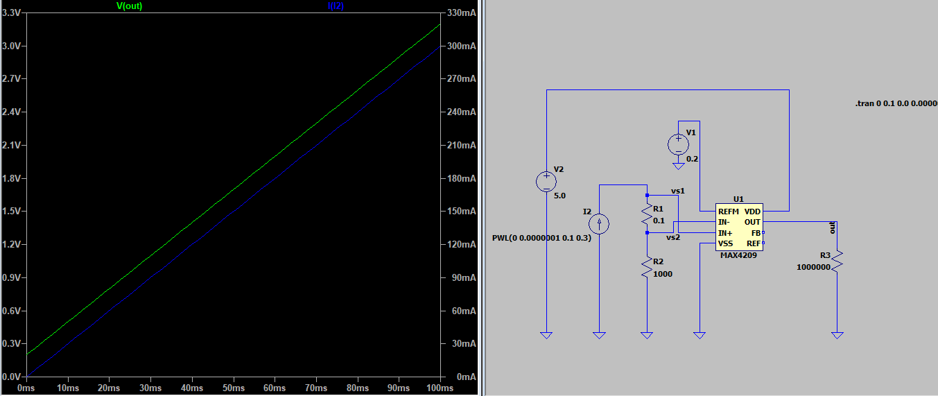
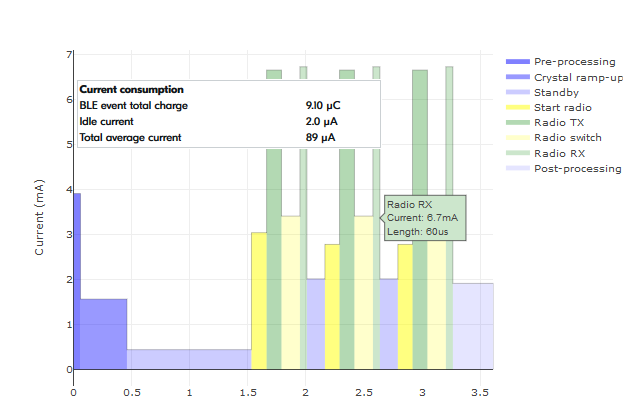
    The shortest current spikes are only 60 microseconds in length, and the idle current when the radio is not active goes down to 2.0uA. I don't think it is necessary to measure nano-amps of current, it might be important for systems using coin cells, but for systems with rechargeable batteries it is enough to know that the quiescent current is ~<5uA.

    In contrast to the nrf52, which is optimized for low power operation, your typical arduino program will use ~50mA - even if it isn't doing anything. Here is a power sample from a very simple arduino program that is just polling a magnetometer and feeding the data out to a serial port.
    For systems with motors, large displays, or lots of LEDs, even higher ranges would be necessary, but I don't think it is going to be possible to design a single system with a dynamic range from 5uA up to 1A. For now I am just going to focus on the 5uA to 100mA range.

    My first inclination was to use a current sense amplifier (sometimes called current monitors). As the name implies, the are specialized instrumentation amplifiers designed specifically for measuring high-side currents (measured above the system load) developed across shunt resistors. The cool thing about current sense amplifiers is that they can measure common mode voltages that exceed their supply voltages. This means that you can have amplifiers like the TSC101 that can measure common mode voltages ranging from 2.8V to 30V even when supplied by only 4V. This dark magic allows you to put your sense resistor above your load instead of putting it down next to ground.

    The problem with current sense amplifiers is that they have huge dead-zones at low input voltages. For example, check out this plot from the TSC101 datasheet.

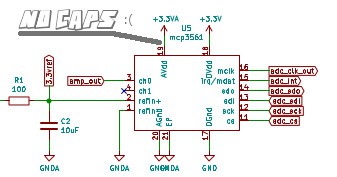
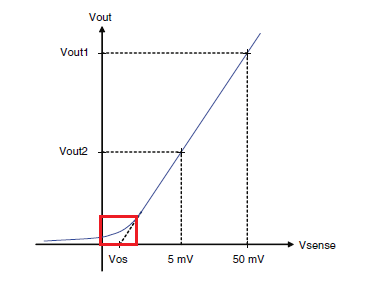
    The voltage listed here as Vsense is the differential voltage measured across the shunt resistor. Between 5mV and 50mV it looks awesome, but the lower the voltage gets the more uncertain the measurement becomes. This error is the result of the amplifier offset voltage. The higher the offset voltage, the worse the amplifier will be at measuring low currents. This particular amplifier has a nominal offset voltage (labeled Vos in the figure) of 0.2mV at a temperature of 25degC.

    That means that if I were to use a 50mOhm shunt resistor,  at a current of 5uA, the the sense voltage would be 250nV. The offset voltage is 200000nV, so there is no way that we would be able to measure the current accurately. I could (and probably will) use a larger shunt resistor, but even if I were to use a 1 Ohm resistor, the sense voltage would be 195uV less than the offset voltage for this particular amp. The takeaway here is the the offset voltage is very important.

    Time to picks an amplifier. Here are some of the options I considered.
    Device
    Vos
    Bw (3db)
    Gains
    cost
    complexity
    TSC101
    200µV
    500kHz
    20,50,100
    $.76
    very low
    MCP6C02
    1.9µV
    500kHz
    20,50,100
    $1.28
    low
    INA233
    10µV
    *
    ?
    $1.5
    high
    MAX9923t
    0.2µV
    50kHz
    25,100,250
    $2.01
    low
    NCS210RSQT2G.55µV40kHz200$.36low

    * the ina233 has an integrated ADC, so the bandwidth doesn't matter. How fast is the sampling rate? Well, it only has an i2c interface, so probably not that fast.

    ** cost is per thousand.

    Annoyingly, the best looking amplifier is also the most expensive one. The NCS210RSQT2G looks pretty good and the price is appealing, but the variance on Vos is much higher than the maxim amp. I might look into the cheap...

    Read more »

  • High level design: picking the essential features

    justinbrowe05/01/2019 at 12:32 0 comments

    Bearing in mind that the goal of this project is to create a tool that makes it easier to debug and optimize devices that need to operate on very low power, I think that the clogger should have at least the following features:

    • The clogger should be able to accurately measure currents down to ~+/-5 uA.
    • It should be able to measure the supply voltage for the device under test.
    • The analog to digital converter should sample fast enough to measure current spikes only 10usec long. It is not uncommon for microcontrollers to turn on peripherals for only microseconds.
    • The amplifier should have a high bandwidth. Signal features lasting only 10usec should not be significantly attenuated. That is going to be tough.
    • The clogger should be possible to feed the amplified current measurements directly out to an oscilloscope (in addition to feeding it out to the ADC).
    • It should be possible to log measurements directly to an SD card.
    • It should be possible to stream average measurements to a computer.
    • The device under test should be able to send markers to the logger.
    • The computer should be able to send commands to the logger to enable, disable, and control features.
    • If it is necessary to have multiple ranges, it should warn users if they are measuring outside the safe range.
    • The power supply input for the device under test (DUT) should be over-voltage protected and reverse current protected. Overvoltage events should trigger warnings visible.
    • The device should have a button to start/stop logging and an led to indicate whether logging is in progress.
    • The clogger should have an LED indicating when it has received messages from the device under test.
    • The clogger should have an LED indicating when it has received a message from the computer.

    There are plenty of other features that would be nice, but not essential:

    • An onboard display showing the average current over the selected time window would be nice.
    • A potentiometer for adjusting the time window on the fly would also be nice.
    • Alternatively, it might be nice to support a bluetooth interface to allow users to check average current measurements using their phones.
    • It would be fantastic to include a high resolution onboard display with a high refresh rate to display real time current measurements.
    • It would be nice if the clogger could operate as a standalone device (without being attached to a computer). That would mean having its own power supply.

    Based on these features, there are really just three main systems: the amplifier, the analog to digital converter, and the controller (which includes the sd card, the led indicators, and all the communication systems).