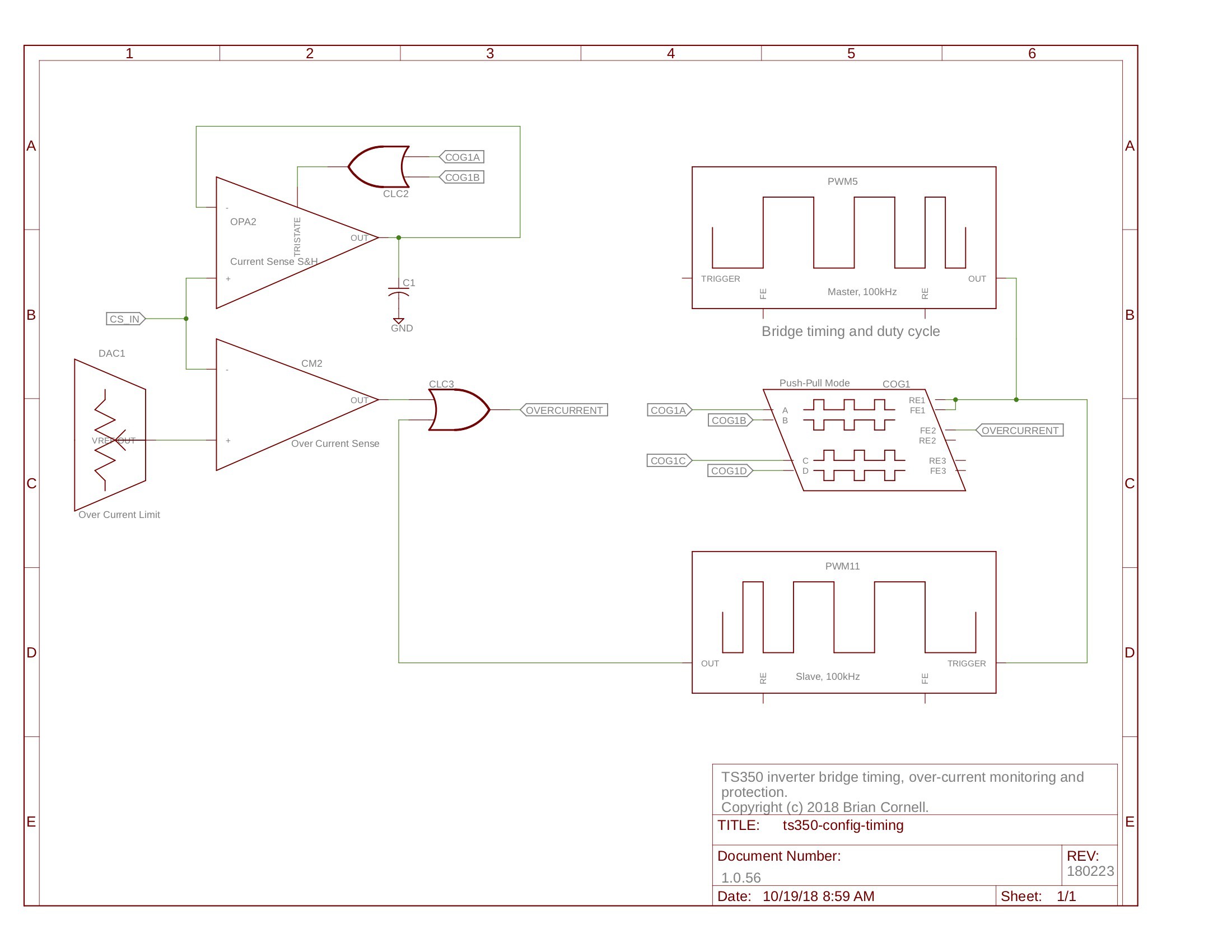
The TS350R1 employs a discrete, high-side current sense circuit in the inverter primary that is the basis for all over-current protection & monitoring in the unit. Reference the main & inverter gate drive schematics for details.
The current signal is derived from a pair of 3mΩ (R302, R303) sense resistors that create a 1.5mV/Amp voltage drop across them. A resistor solution was chosen due to its compact size and low cost. They are placed in a high-side configuration due to the high currents and to provide better protection for the bridge. Low-side circuits can’t detect shorts occurring upstream and can contribute to ground bounce related problems for the gate drivers.
The challenge with high-side sensing is that it isn’t ground referenced so the conditioning circuit must operate from an floating supply or be capable of handling the common mode voltage. Since isolation isn’t practical the TI OPA197 (U2) is used. It allows for rail-rail inputs and supports slew rates up to 20V/uS which is satisfactory for per-cycle current limiting. It is configured as a differential amplifier. R4 & R5 in conjunction with D2 & D3 provide input protection from voltage spikes. R4 & R6 set the gain at 10 and Q1 level shifts the output (removes the CM voltage) for direct consumption by controller U101.
The controller processes the current sense signal to provide per-cycle [SOA] protection for the bridge MOSFETs and to perform overall power management thru two distinct hardware pathways using on-chip peripherals.
MOSFET SOA Protection
Per-cycle protection uses DAC1 to provide a reference voltage to comparator CM2. The reference voltage is set to a value high enough (140A) to support the significant currents required of equipment startup surges but still within the MOSFET’s Safe Operating Area. CM2 compares the sense value to this reference and produces a H->L transition that is gated thru logic cell CLC3 to a Falling Event input of the COG (Complementary Output Generator). A transition immediately terminates the gate drive for that side of the bridge for that cycle.
The role of CLC3, along with PWM11, is to provide a blanking function at the beginning of each half cycle. Blanking prevents a premature termination of the gate drive and is set to a few hundred nano-seconds (defined by the DC of PWM11). This is necessary because of the inherent noise in the current sense signal. Noise is a problem for all sense circuits based on shunt resistors but it is more significant in high current, high frequency applications due to parasitic inductance and poor signal to noise ratios.
Current Averaging
The current sense signal is also connected to the non-inverting input of opamp OPA2 which is configured as a voltage follower. This is necessary because of the relatively high impedance of the current sense circuit’s output and, most importantly, for OPA2’s tristate feature. Tristate, along with C1 (C102 on the main schematic) form a sample & hold circuit that averages the current sense signal from both sides of the bridge and allows the controller to derive RMS current. CLC2 gates OPA2’s output to ensure that it is only passing a signal when the bridge is active.
The voltage read from C1 represents an averaged value of the sense signal but it reads high. This is because the sense circuit delivers an exaggerated slope with a large spike (parasitics) at the end of each cycle which inflates the measured S&H voltage. Since the controller has limited processing bandwidth a linear coefficient is applied to reduce the read current to obtain a value that is +/- 1.5A of the actual RMS value.
The controller multiplies this RMS current value with the inverter’s input voltage to estimate the input power and uses this to perform load management. The power value drives the front panel LED meter and overload shutdown.
Overload and Power Management
In this design current, much more than power, is the most important parameter to watch for unit protection. That said, it manages by power because this is the better metric for the entire unit over its input voltage range. With a 15V input and 80% efficiency the input power is:
Po / n = Pi -> 350 / 0.8 = 437.5 watts (1)
And the required input current is:
Pi / Vi = Ii -> 437.5 / 15 = 29.16 amps (2)
Whereas at 11 volts the required input current is:
437.5 / 11 = 39.77 amps (3)
So if the load was managed by current alone and 33A was the expected full load current, a 15V input at that current would be delivering:
(Ii * Vi) * n = Po -> (33 * 15) * 0.8 = 396 watts (4)
And an 11 volt input would only be delivering:
(33 * 11) * 0.8 = 290 watts (5)
Higher input voltages aren’t a concern because the sine section can easily handle in excess of 400 watts continuous. But, at low voltages there is the risk that the inverter will overheat due to high currents and create user confusion since the power meter won’t display a full / boost load. This is solved by derating the inverter below a set-point input voltage (Vsp) using the concept of equivalent power (Pe). This approach maintains a unified control loop based on managing by power.
The set-point refers to an input voltage that is reasonably expected to be available in the real world - e.g. automotive 13~13.8V and that the inverter can supply rated power with some operating margin for boost. Equivalent power is defined as the actual power when operating above the set-point and, when below is:
((Vsp - Vi) * Ii(rms) + Pi = Pe (6)
The controller uses Pe to drive the load meter and for overload protection. It also calculates the actual input power and that value can be accessed thru the service port.
Over Current Protection
Over current protection is different from overload. It is intended to disable the inverter when the per-cycle (SOA) protection engages repetitively over short time intervals. This indicates either a failure in the bridge or sine sections or excessive current being drawn from the AC load.
Detection is done by measuring the duty cycle (DC) of the inverter using the controller’s Timer5 peripheral. Since DC is a constant value, anything less is considered an over-current event. The controller’s run-time loop samples the DC continuously and applies a simple PD (proportional derivative) algorithm to disable the inverter if the frequency or rate of events exceeds a set limit. This approach is used to support short duration (<2mS continuous) inrush events typical of AC equipment and allows in excess of 20A to be sourced.
Sine Current and Load Protection
As described above, the main controller provides load management for the entire unit. Current protection is passive and works for several reasons.
- The output filter inductors, L401 & L402, limit the di/dt imposed on the sine bridge transistors.
- There is limited instantaneous energy available in the high voltage supply capacitors C407, C408, C410.
- The SOA envelope of the sine bridge MOSFETs.
- The relatively high impedance of the inverter, in part due to its active current limiting.
A picture, instead of a mathematical analysis, best summarizes these points.
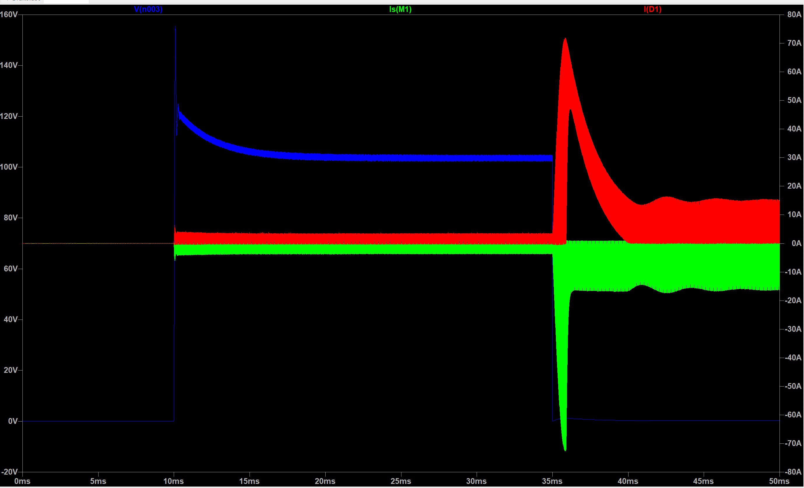
This is a spice simulation of a dead short event on the sine output. The blue trace is output voltage, green is current at the MOSFET source node, and red is the cathode of the freewheeling diode. The output is turned ‘on’ at 10mS and runs at full load until 35mS when the output is shorted. The large current spike is the bulk capacitance discharging.
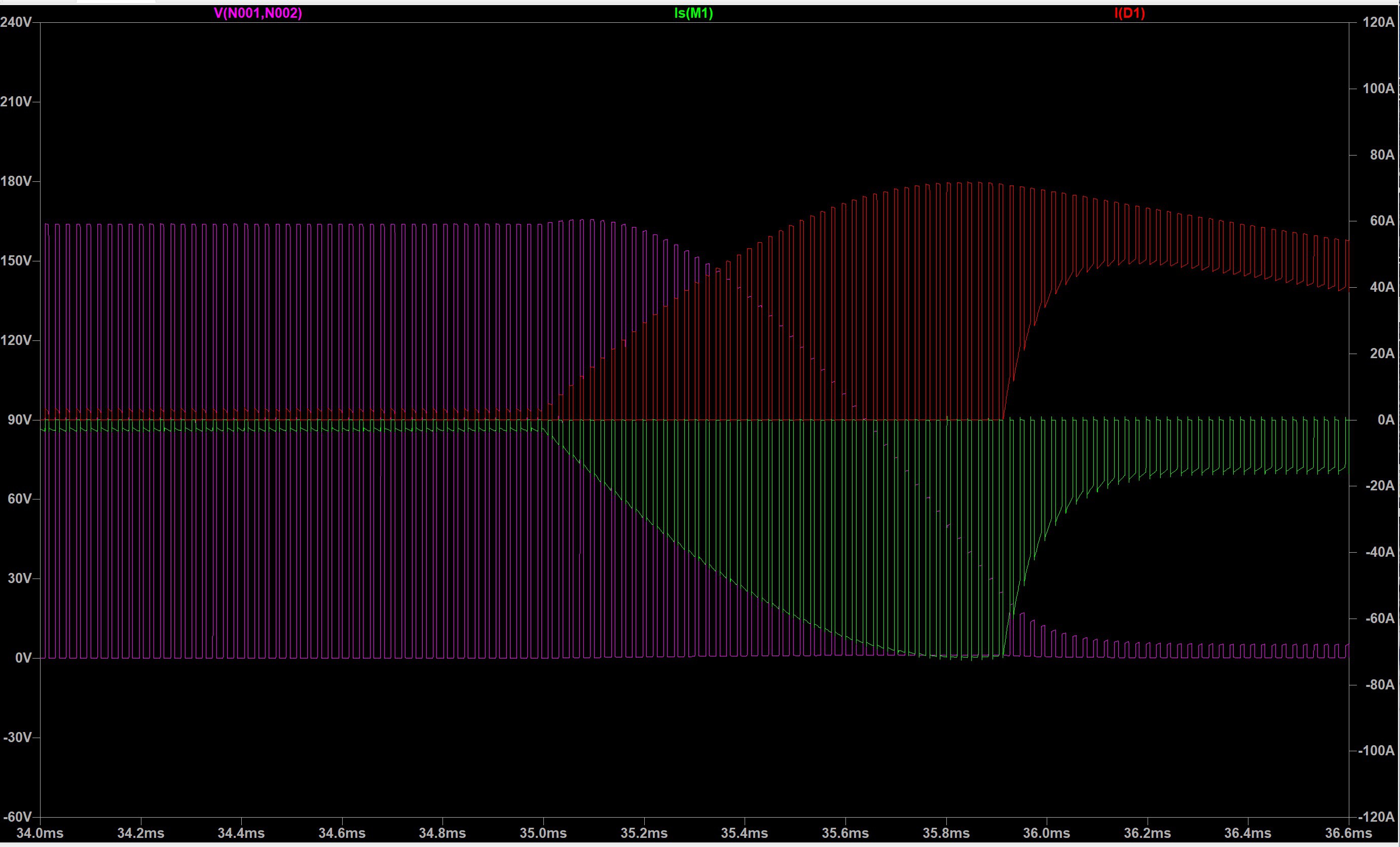
Zooming in on the start of the event, you can see that the drain to source voltage (magenta trace) is well below 100V before peak current is reached. The actual peak currents will be lower due to capacitor ESR, DC resistance of the inductors, Rds(on) of the MOSFETs, and the inverter’s impedance (which is higher than represented in the simulation).
Here is the simulation circuit.
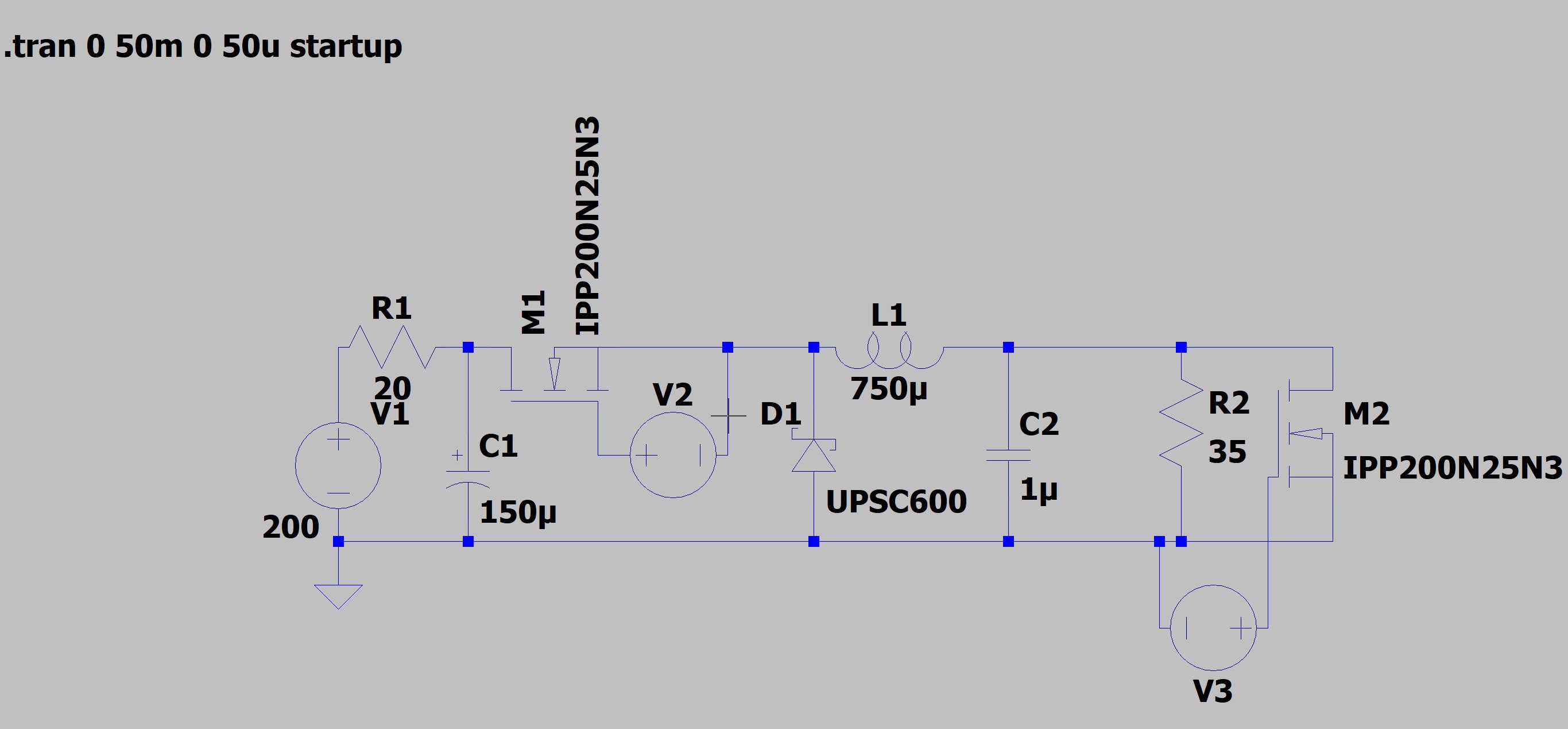
V1 and R1 form a limited impedance voltage source. M1 and D1 simulate one half of the sine bridge with D1 functioning as the low side MOSFET. C1 is the bulk capacitance. V2 is the floating gate drive set to a 63% DC which is the average over a half sine. L1 and C2 represent the output filter with L1’s value set to the expected inductance at full load. R2 simulates a 3A load, and M2 and V3 form the shunt which triggers at 35mS.
Last, the transistor’s Safe Operating Area is an important selection criteria:

The FDP20N50 can handle 30A with 300V across it for ~ 100uS and, as voltage decreases the current handling increases to 80A. More than sufficient.
This simplicity does have a shortcoming: it will not protect the sine bridge from an internal short. The absence of this protection isn’t a safety issue, so it was omitted to retain a simple & cost-effective design.
Discussions
Become a Hackaday.io Member
Create an account to leave a comment. Already have an account? Log In.