 Maave
MaaveI received my PCBs and components. I tried to assemble. I failed. The flex PCB and QFN parts were more challenging than I expected and I botched soldering the atmega and FFC connector. Rather than sink more time into an early design, I've decided to cut my losses and continue to v0.2. I could complete v0.1 with the help of a friend however v0.2 has so many changes and v0.1 has several flaws (not dealbreakers but annoyances) that I think my time is better spent moving on.
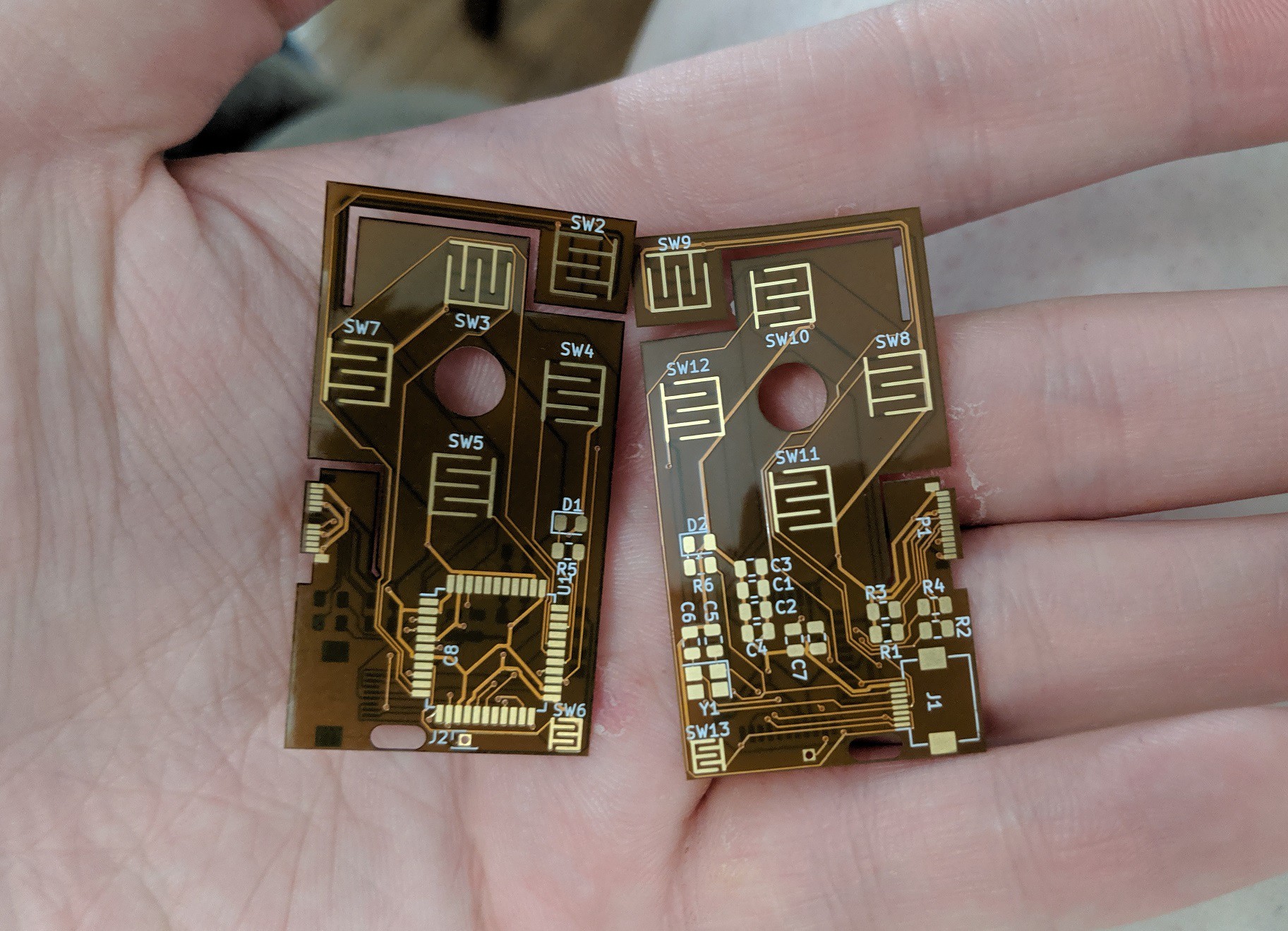
Fresh PCBs
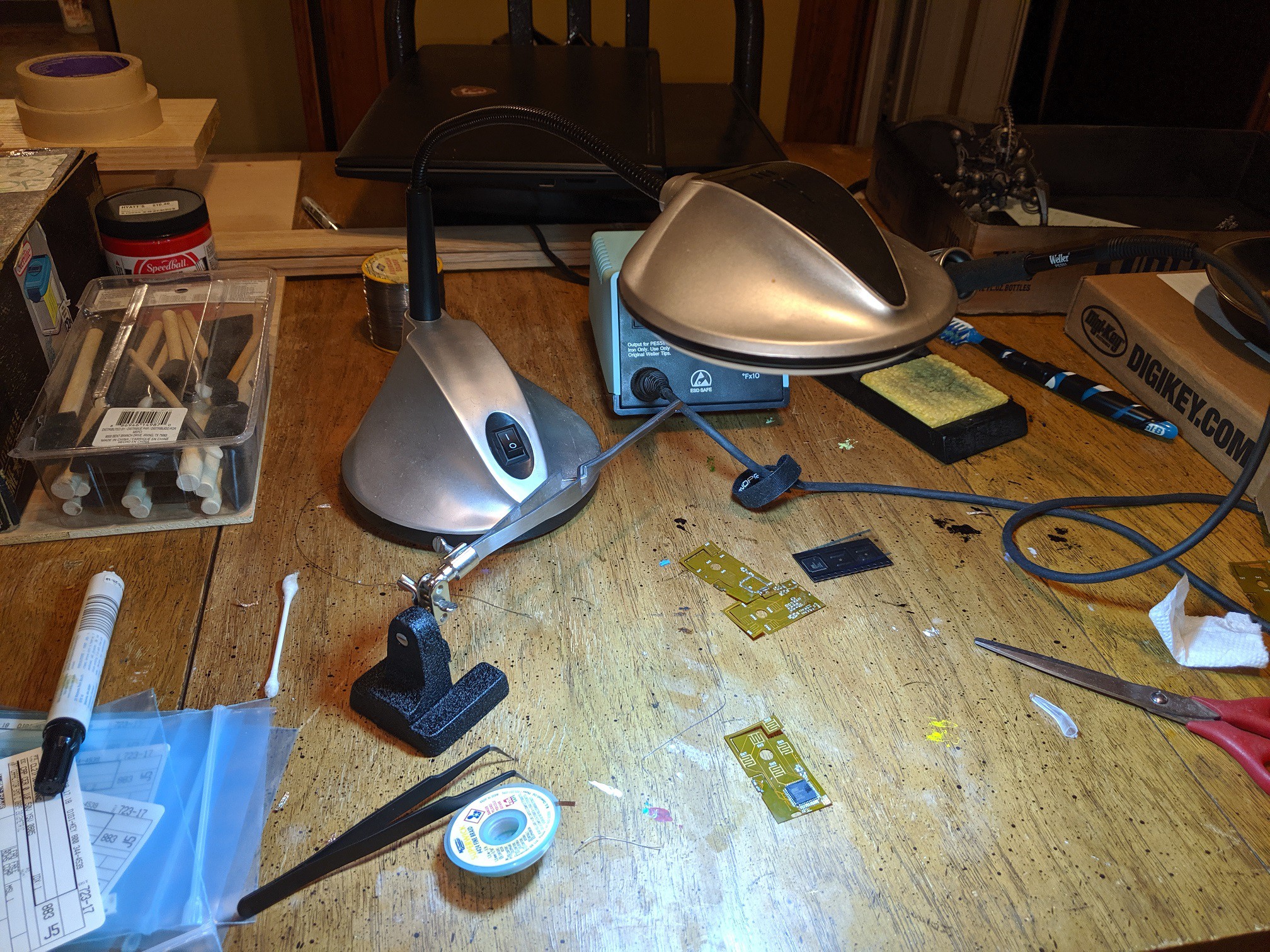
The craft table. This LED light is the best thing ever. Light is so important for seeing small details. The next upgrade will include magnification.
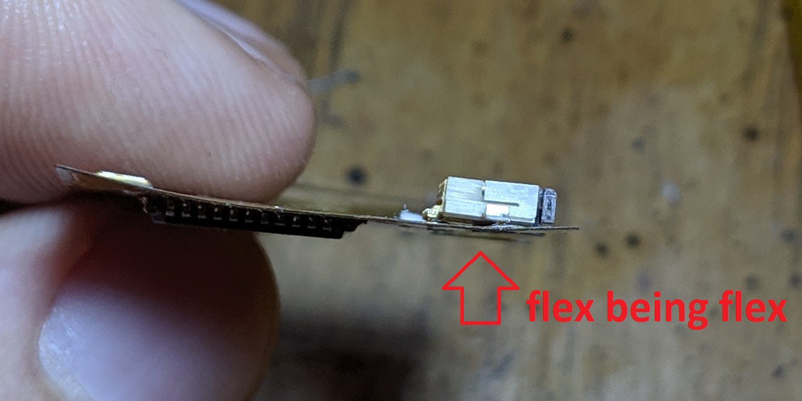
An example of flex being a pain in my butt. The board is flexed and creates too much gap to solder properly.
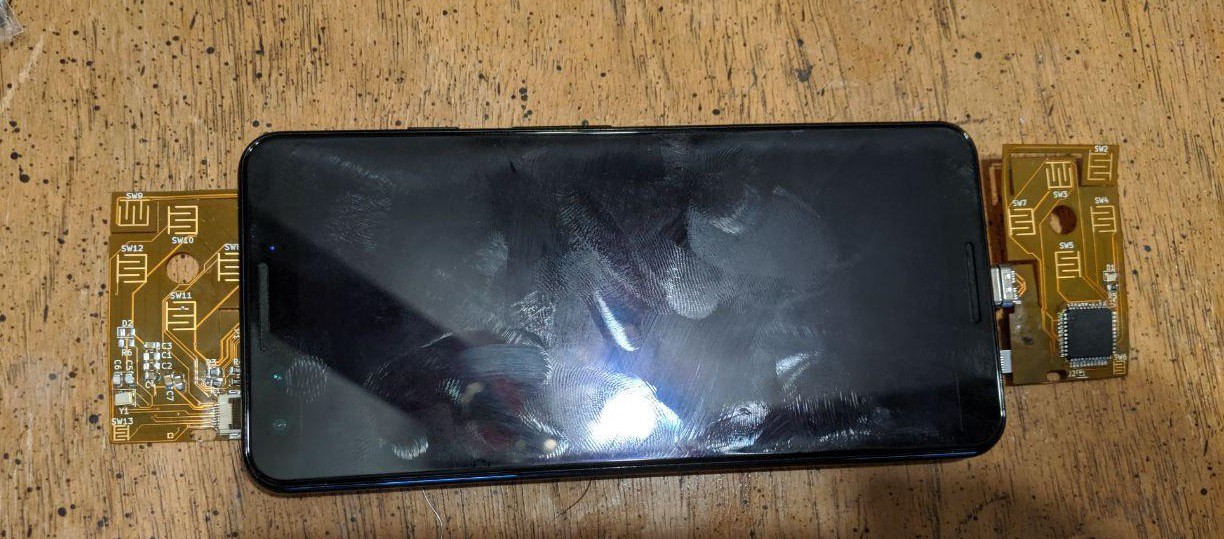
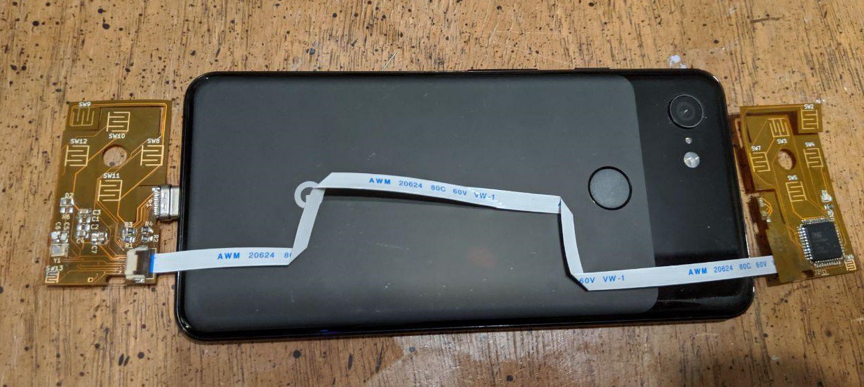
Here are 2 boards connected and mocked up on a phone.
The FFC is very flexible. It can handle one-time bends too. This gives me more options.
Lessons from v0.1:
- review instructions before attempting new soldering techniques
- use the right tip (mine was too fine and I couldn't find the spare)
- tape down flex boards
- the flex trigger works well
- you can't hold flex PCB in alligator clips. It bends the PCB which misaligns pins/pads. Taping it to a hard surface works.
- attaching the USB-C connector (meant for 0.8mm FR4) to the thin flex was a bad idea (I knew this but wanted to try anyway)
- read the datasheets, I wired a 4-pin crystal wrong (could be kludged)
- the USB-C connector sticks out more than expected
- the FFC cables are very flexible and easy for a user to install
- reusing the same board for both sides of the phone complicates the routing
- reusing the same board increases the board size, negating some of the benefit
- the yellow flex PCB is kinda ugly and would limit art
- components on both sides are annoying to solder (I knew this but wanted to try anyway)
- why didn't I put debug pads on this?
- my "space saving" reset button is difficult to use in practice
Let's take a look at v0.2 (not final).
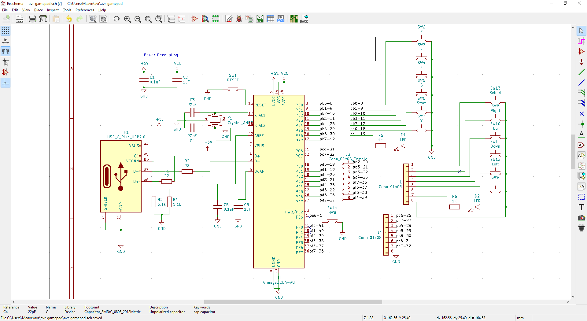
Changes for v0.2
- flex features have been removed
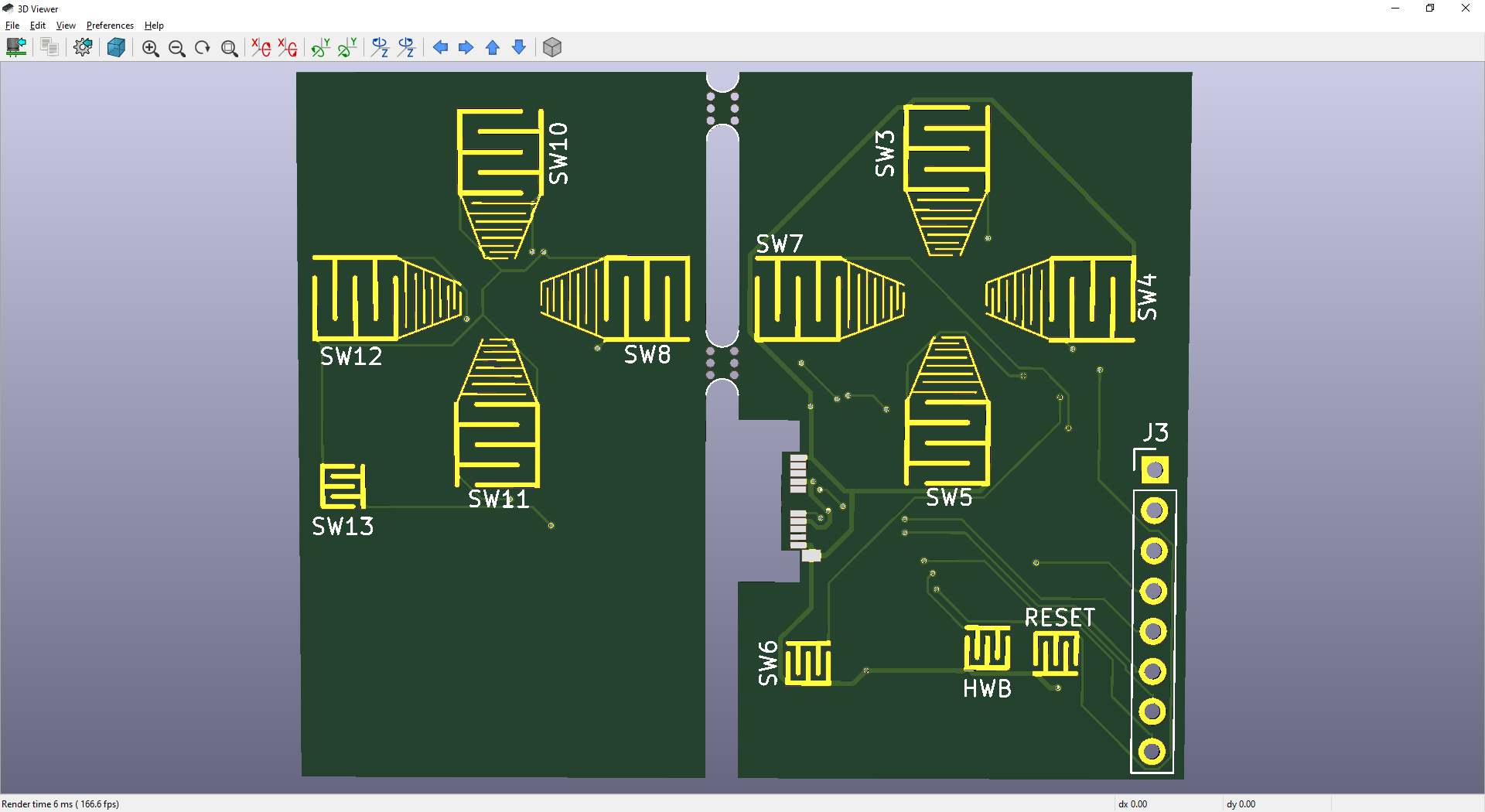
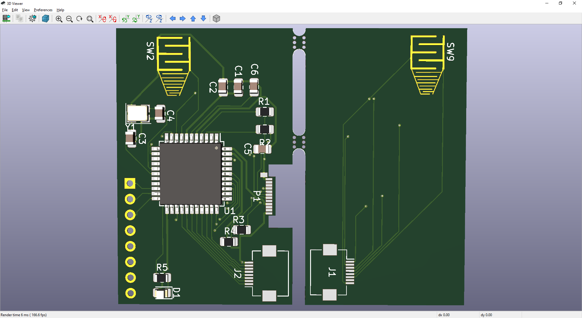
- moved all components to one side
- the trigger will hinge, similar to the Switch trigger. This simplifies the PCB but complicates the case
- the double sided feature (reusing the same board for both sides) is gone
- a few 0.1" standard headers are added, connected to some digital and some analog pins
- USB-C connector has been recessed so the PCB sits closer to the phone
- the face pads have be reshaped to accommodate silicone buttons from multiple controllers
- plans to use Switch Lite silicone and buttons as soon as they're available aftermarket
- added simple PCB art
- crystal wiring has been fixed
- FFC location has been fixed so I can use straight-through FFC
My roommate got a Switch Lite and the buttons are excellent. They're firmer than the DS or PSP face buttons, the buttons sit a little higher, and I can feel the rubber dome collapsing (unlike the PSP face buttons which are mushy, there's not much tactile response). These are the best handheld console buttons I've felt yet and they'll work perfectly in the controller once more aftermarket parts are available.
The headers are intended for debugging, programming, and testing future features like analog joysticks and audio output. However I realized that they could be an attractive feature. This is the first atmega32u4 breakout I've seen with a male USB-C connector (the Elite-C and Goldfish have female USB-C). This could open the door to other DIY phone accessories.
v0.2 is almost ready and the PCB will be ordered soon. I've recruited the help of my friend [ldrrp] to ensure 0.2 works the first time.
Discussions
Become a Hackaday.io Member
Create an account to leave a comment. Already have an account? Log In.