 Ted Yapo
I started with an ambitious project, optimizing an SMA connector footprint, but had to scale back to get a better understanding of how this all worked. It turns out that a lot of my experience in lower-frequency regimes and SPICE simulation can be fairly misleading :-)
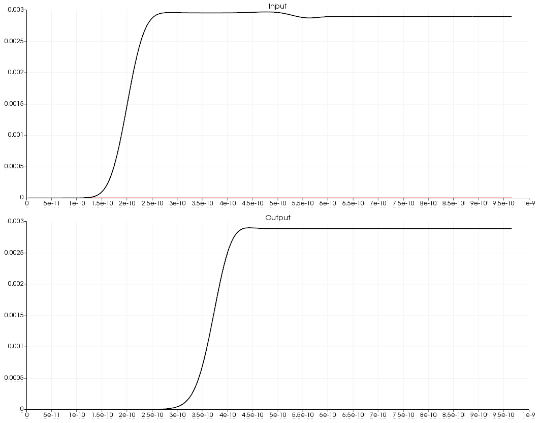
The simulation shown in the video is of a 1-inch piece of microstrip 109 mils wide on a 2-layer PCB with 60 mil FR-4 - it's the OSH Park 2-layer stackup. There are two 50-ohm ports, one on each end. A 20-ps rise-time Gaussian step is applied to the input port. The animation is of the magnitude of the electric field in the FR-4 substrate.
You can see apparent overshoot in both ports, then later a reflection arrives back at the input port. It turns out that these overshoots are a result of exciting high-order propagation modes in the microstrip. We tend to think of microstrip as a type of "flat coax" which operates in TEM, but that's not right, I have come to find out. It turns out that because the dielectric is only on one side of the conductors, microstrip supports other transmission modes , which can be especially troublesome as the thickness of the dielectric approaches a significant fraction of a wavelength.
The problem here is that the 20-ps rise-time edge has frequencies high enough to excite these other modes. If you drop the rise-time down to a more reasonable value of 70 ps, for example, you get the following:
Much better. You can still see the effect of a reflection in the input port trace. This is a reflection from the output port that has made its way back to the input port. More problematic than the reflection itself is the different levels before and after the reflection. This is caused by the fact that the impedance of the trace isn't exactly 50 Ohms. Interestingly, this 109-mil wide trace was created by the PCB calculator that ships with KiCad. It's not quite right.
After some experimentation, I ended up with a 117-mil wide trace. You can see the difference in this plot, where there still is a reflection off the output port, but the levels are the same before and after, indicating a good impedance match.
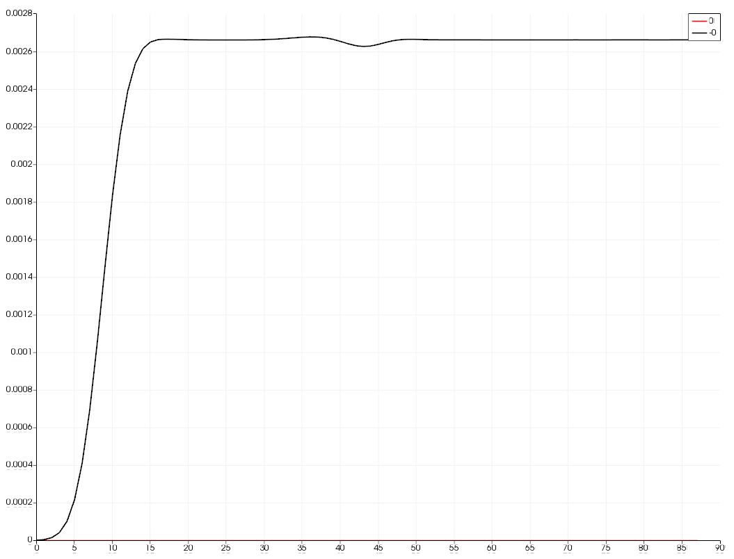
The fact that the reflection is still present is an artifact of the port geometry. In this case, the ports are simply 50-Ohm resistors as wide as the trace on either end and connected, through the substrate, to the ground plane. This isn't a perfect termination, and creates reflections. There are some improved terminations in the literature, but none of them looks particularly easy to implement in this case.
I may experiment a little with some improved terminations before continuing with more complex models. It would be useful to have a good one available. It would also be useful to simulate some real-world terminations to see how they perform. I have an intentional AC-short termination in one of the designs in an earlier log, and it would be interesting to see how it could be improved.
At least I got something going. Next, I may move to a coplanar-waveguide structure. I don't know how to connect the top and bottom ground planes to get a good launch, so some experimentation will be in order.
I'd also like to experiment with adding soldermask. Unfortunately, I'm not sure how to make a conformal coat easily - although I have a few ideas. It seems like it's worth trying, if only to simulate and verify the results I saw on real PCBs.
Discussions
Become a Hackaday.io Member
Create an account to leave a comment. Already have an account? Log In.