FuzzyNoodle
When I am building a biped robot, I was always thinking of having some sort of cool gadget that can trace my opponent and do attack moves with it. Bunches of radar/lidar projects already exist here. However, there are some limitations for my purpose:
- Ultrasonic wave sensor modules are quite large. Every robot would look like WALL-E.
- Current radar projects all includes a sensor (either ultrasonic waves, IR, laser, ...), and a servo motor in the middle. Scanning the environment requires the servo to move side to side. Moving stuff back and forth creates momentum changes, which is bad for biped balancing and walking.
- Scanning frequency is limited by servo speed. Only several hertz can achieved, probably. Even if the scanning frequency can be ramped up by some super-servo, this would result in heavy vibration.
- [Central servo motor - sensor] arrangement also limits the position for mounting and the design. It is difficult to mount such thing other than as a head. Which makes my biped look like a shaking-head WALL-E every time. Not cool!
- The [servo-sensor] arrangement can also be built as a [motor-sensor] style. The sensor (or sensors) is rotating along a motor axis continuously. This may eliminates the momentum jerks and low scanning frequency problems, but not the torso design limitation. Wiring difficulty would also increase substantially.
After searching, this tiny sensor VL53L0X from ST splashed into my eyes. By claiming "World Smallest" time-of-flight ranging sensor, the dimension is only 4.4 x 2.4 x 1.0 mm. Featuring
- On chip IR laser emitter and detector
- Up to 2m range (1.2m in fast mode)
- Programmable I2C address
- A GPIO interrupt output pin
- Eye safe
All these special features combined enabled me to overcome the problems above, if an array of VL53L0X sensors could work. Originally, I thought this radar would be called solid state radar, but found out that this term was used for something else. Therefore the "Stationary" word in the title means that there are no moving parts in this radar gadget. Also, while LIDAR (light detection and ranging) is the technically correct term for this chip, RADAR is referred here as a more generic term.
The reason why Programmable I2C address and GPIO output pin are critical to this project is explained later.

Tools
The following tools are required in this project:
- Soldering iron
- Soldering helping hands
- Dupont crimp tool
- 1.5mm hex driver
- Wire coating removal tool
- Wire cutter
- Hot glue gun
- Tweezers
- Magnifier (physical or apps in your phone)
- Flat nose pliers
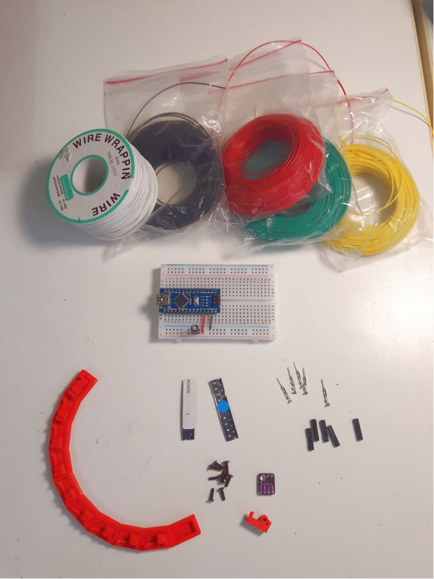
Parts
The following parts are used in this project:
- 10x VL53L0X GY-530 breakout boards
- An Arduino (Uno, Nano, Mega, Zero, Mini, ...etc)
- A breadboard and some breadboard wires
- AWG #26 wires with different colors
- AWG #30 single core wire
- 5x Dupont male connectors
- 5x Single pin Dupont housings
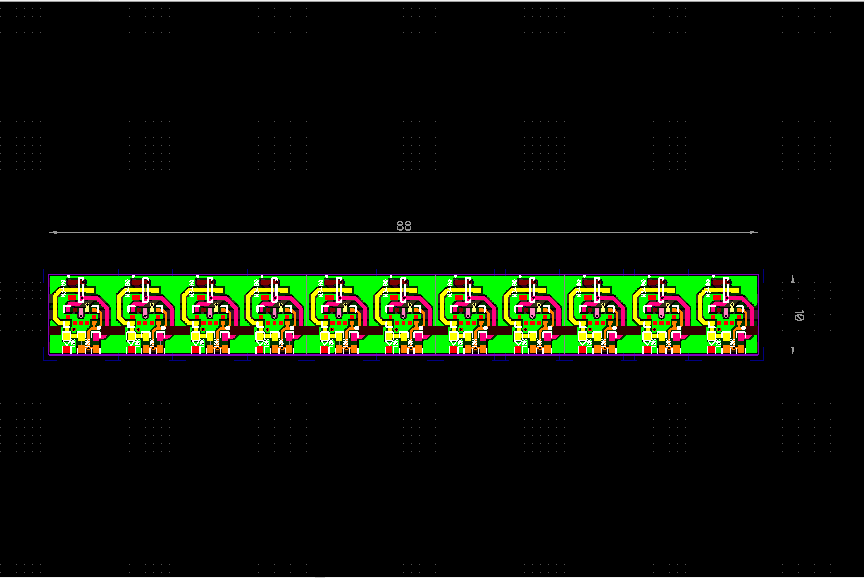
- 10x 3D printed breakout board holders
- 1x 3D printed circular frame
- 10x M2x10 flat head screws
- 10x 0804 LED(Blue reommended)
- 10x SOT-23 AO3400 N-Channel MOSFET
- A small capacitor (10~100uF)
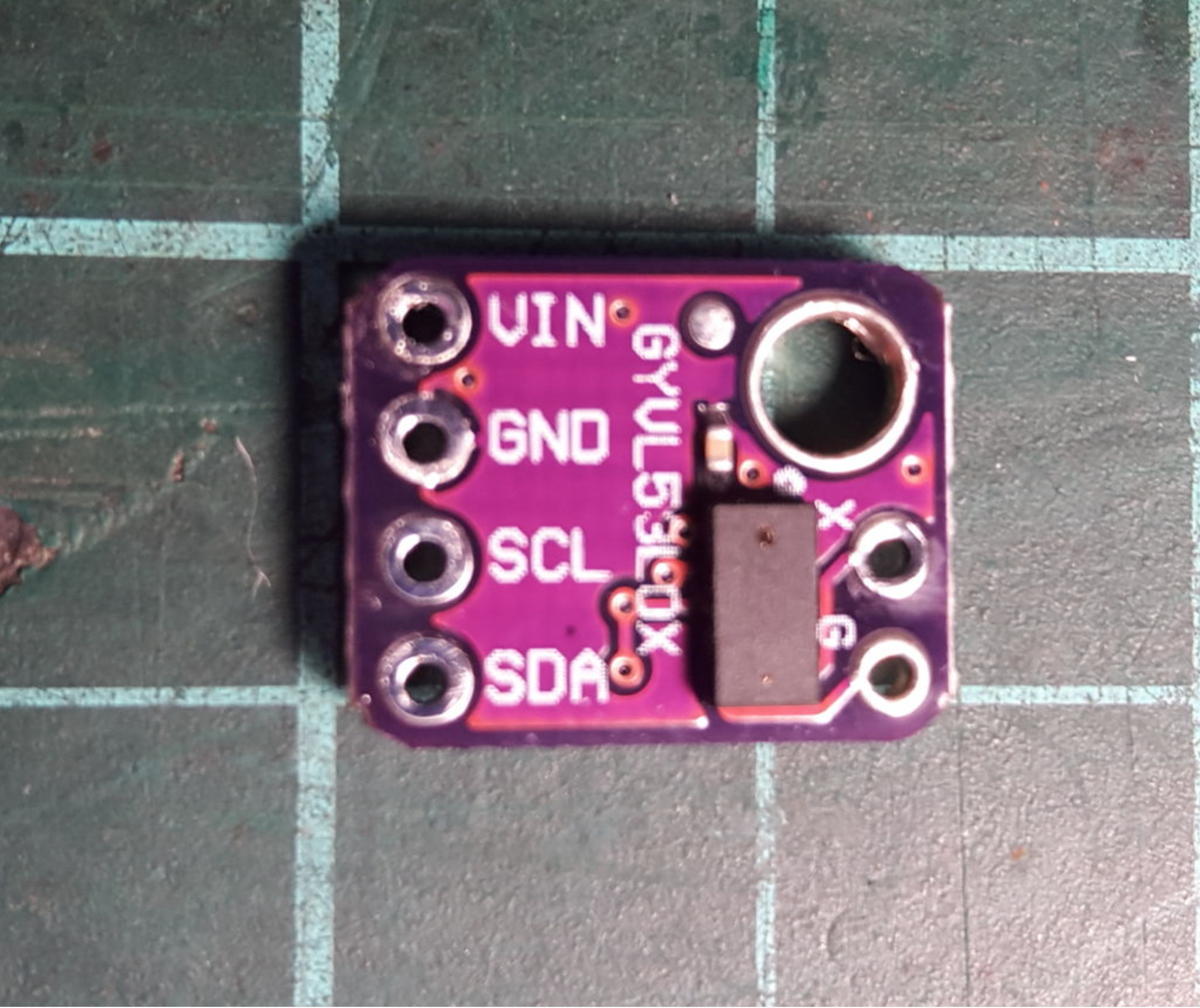
Breakout board
The VL53L0X breakout board I used is GY-530. There are also Adafruit version and Pololu version available. If feasible, I do recommend using Adafruit or Pololu's product because they make great products, great tutorials, and great software libraries. I tested on Adafruit's VL53L0X library and used a modified version of Pololu's VL53L0X library.
Dupont connectors
The dupont connectors are used for the breadboard. You may use any other types of connection you have in hand.
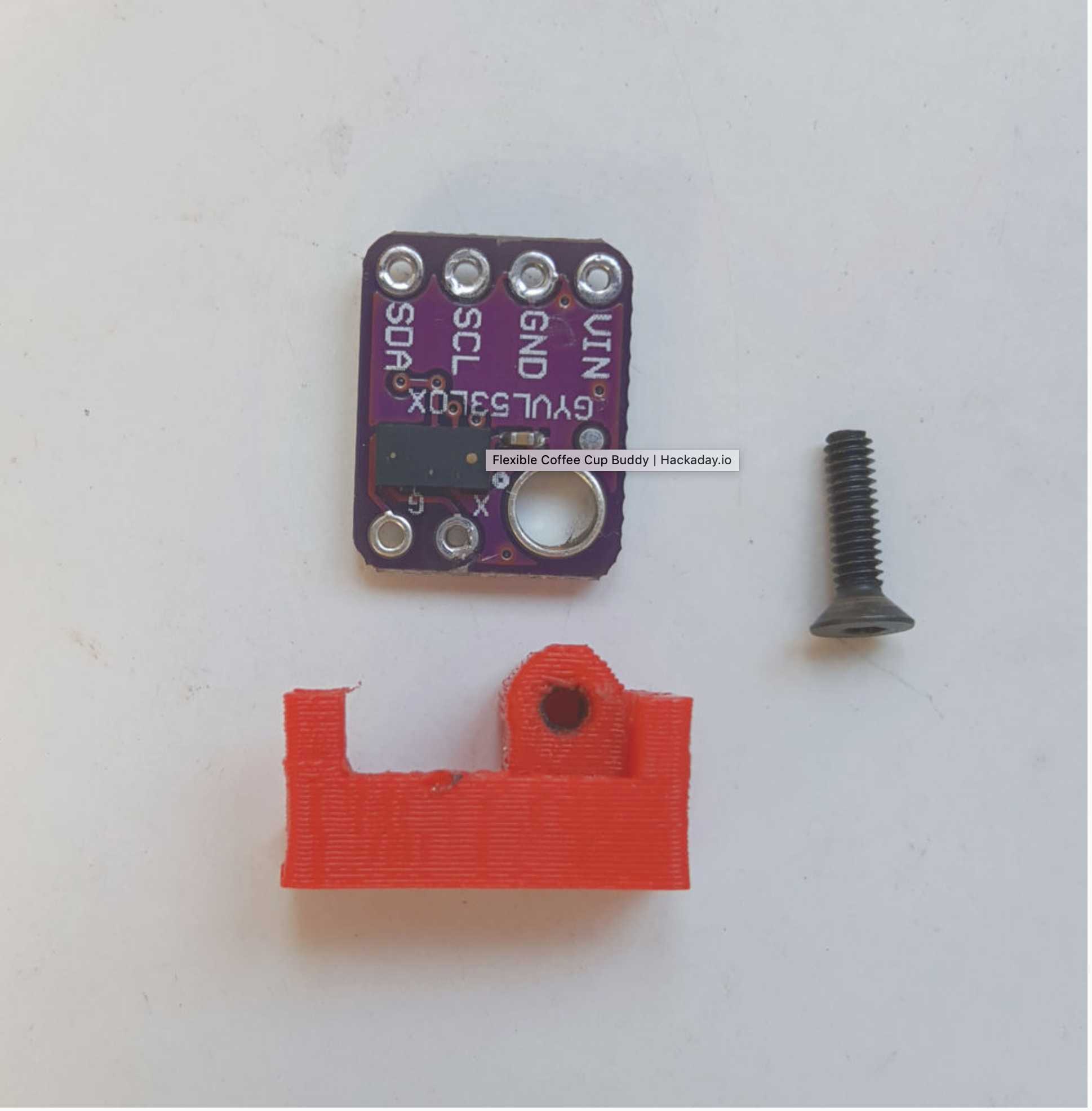
Screws and 3D Printed Parts
The M2 screws, holders and circular frame are used to place the sensors in a circular arrangement. You may use any other methods, such as using card boards, model woods, clay, or even hot glue them on a can.
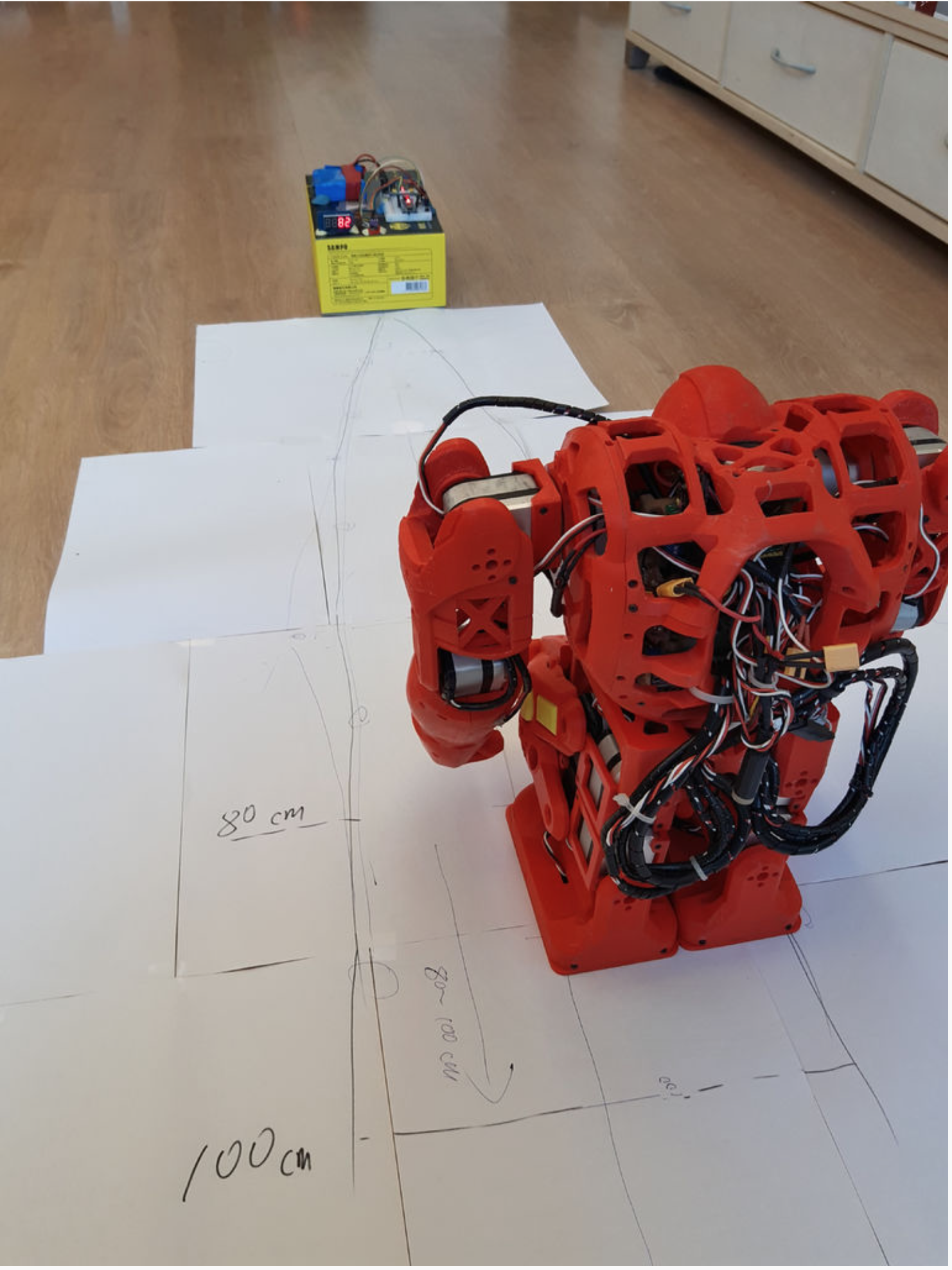
Cone of Detection
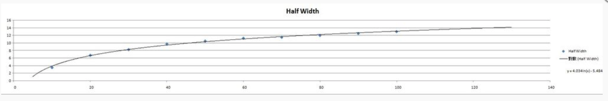
I used a single module to draw the cone of detection. Using a mostly 3D printed robot as the target. The distance are shown on the led display, and measured roughly. The measured data is recorded into an Microsoft Excel file, and used the curve fitting function. The best fit is a natural logarithm curve, with effective distance from 3 cm to approximately 100 cm.
At 60 cm, the detection curve for a single sensor is about 22cm. With a 20 cm wide target, a circular separation of 10~15 degrees for the radar array should yield an acceptable scanning resolution.
I2C Address
While the VL53L0X I2C device address is programmable, full control of the XSHUT pin by the micro-controller is required. The sequence to do so is:
- Power is applied to AVDD.
- All VL53L0X chips are brought to Hw Standby (reset) state by driving ALL their XSHUT pins to LOW.
- Each chip is taken out of reset state one at a time. The default I2C address after booting is 0x52.
- The chip address is changed to a new address through a I2C command. For example, 0x52 changed to 0x53.
- Repeat step 3 and 4 for all chips.
Theoretically, maximum 126 units can be drove in the same bus for the 7-bit address range. However, in practical, bus capacitance and sinking current limitation of the micro-controller may/should limit the maximum device number.
The new I2C address is not stored in the VL53L0X chip against power down or reset. Thus this process has to be done once upon every power up. This means one precious pin is required for every unit in the radar array. This is way too unfriendly to wiring and pin-consumption, for a radar belt with 10+ or 20+ units.
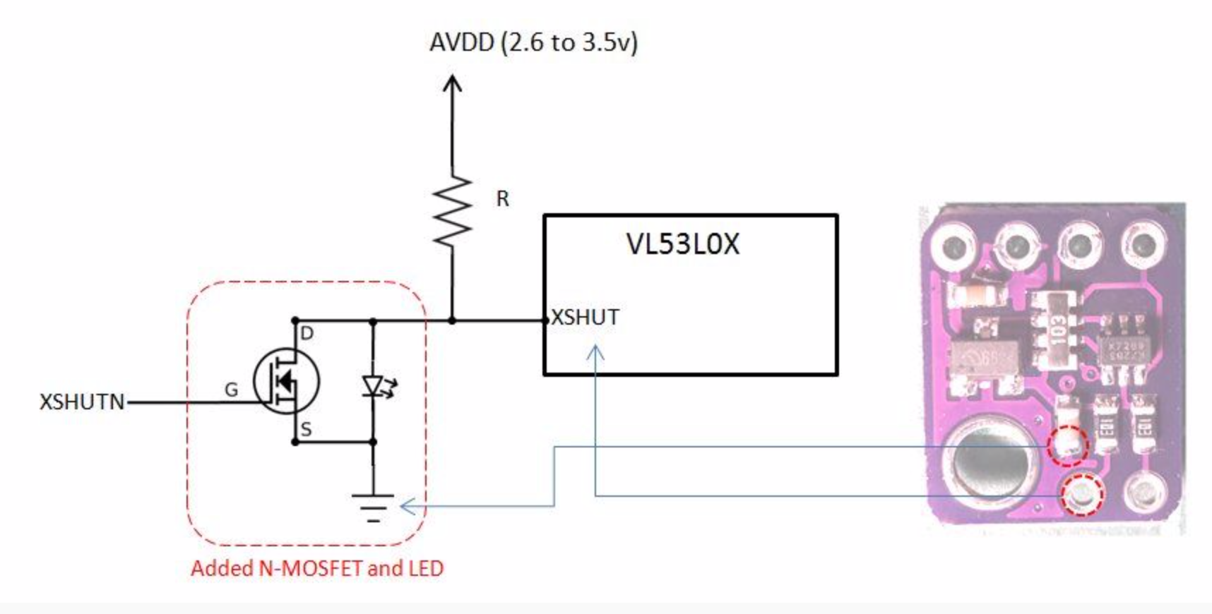
As mention in STEP1, it is lucky that there is a GPIO1 pin on VL53L0X chip, originally used for interrupt, can do the job.
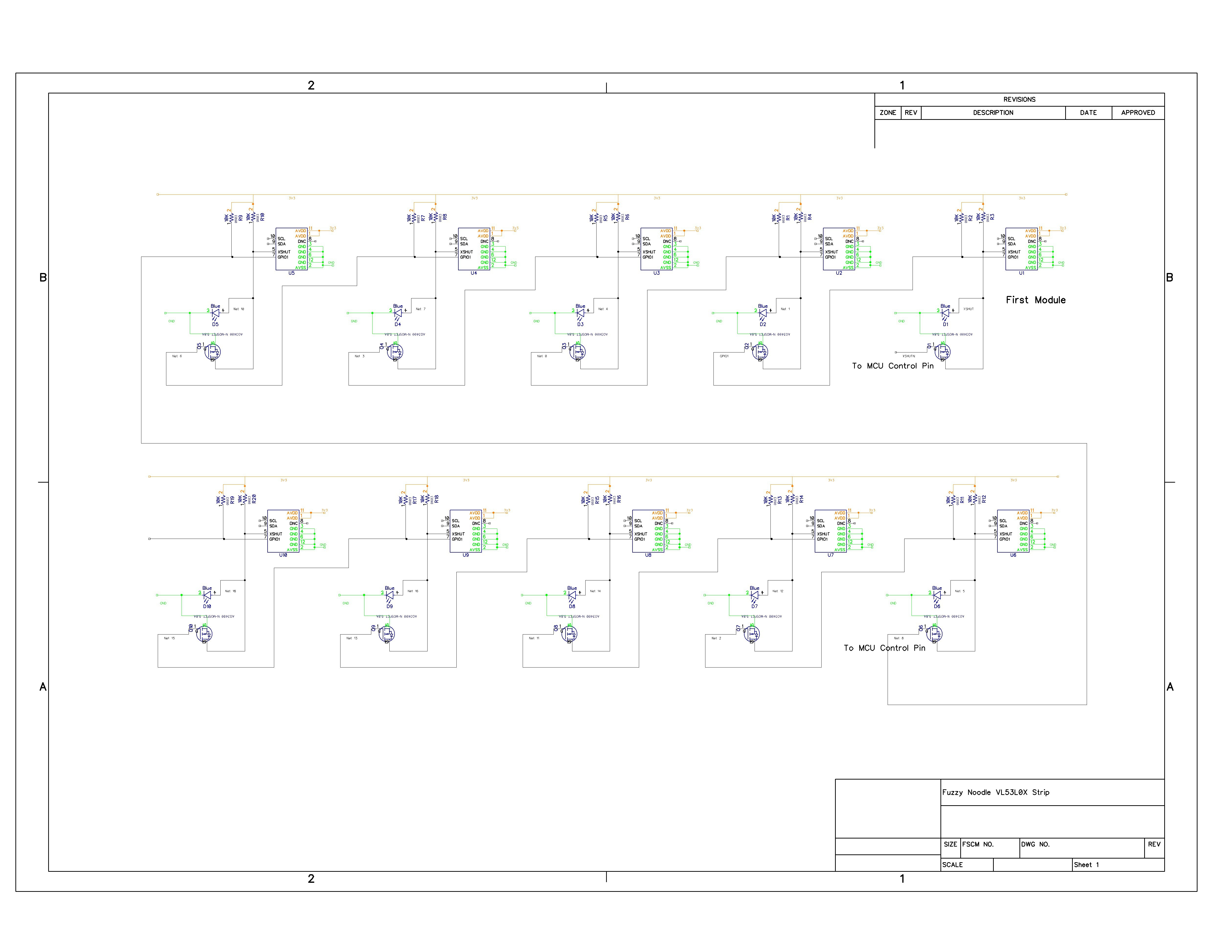
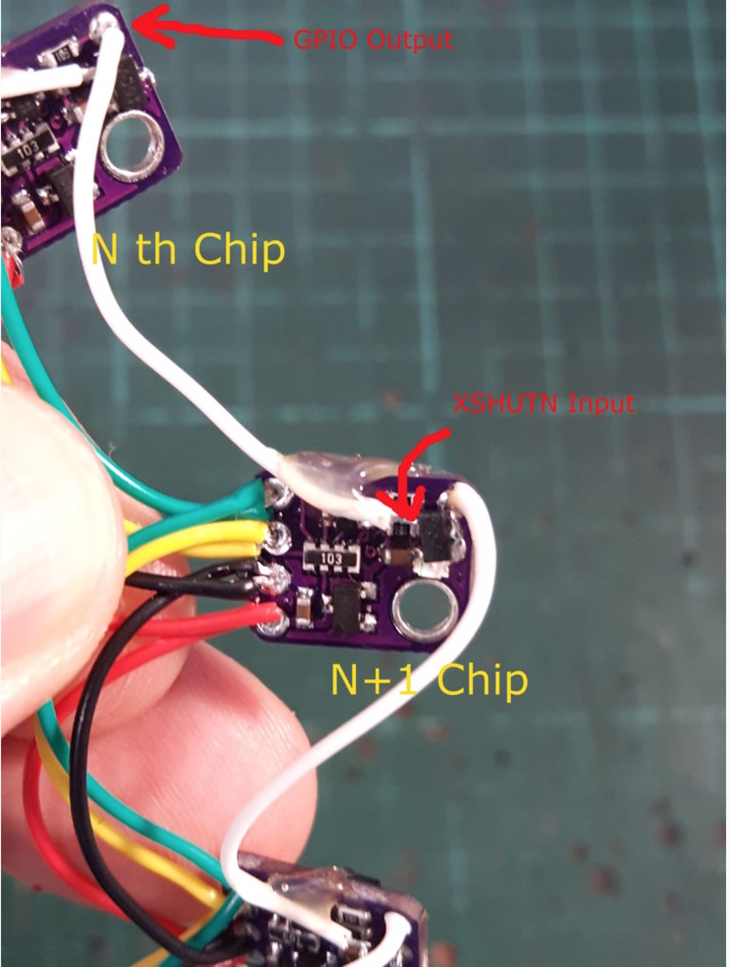
GPIO-XSHUTN daisy chain
The GPIO output is in high impedance state upon booting and open drain to low while active. The GPIO and XSHUT pins are pulled high to AVDD on the GY-530 breakout board, as recommended in the datasheet. To reliably put all VL53L0X chips into Hw Standby state (driving XSHUT low), we need a logic NOT gate (inverter) for every XSHUT pin. Then we connect the GPIO output of one chip (the Nth chip), to the XSHUTN (XSHUT-NOT) of the downstream chip(the N+1 chip).
Upon power on, all GPIO pins (inactive) are pulled up, all subsequent XSHUT pins are drove low by the NOT gate (except the very fist chip where its XSHUTN pin is connected to the micro-controller). The I2C address change and XSHUT release of the downstream chip is done in software, one by one.
If you are using different breakout boards, you need to make sure if the pull-up resistors are in place or not, and make appropriate adjustments.
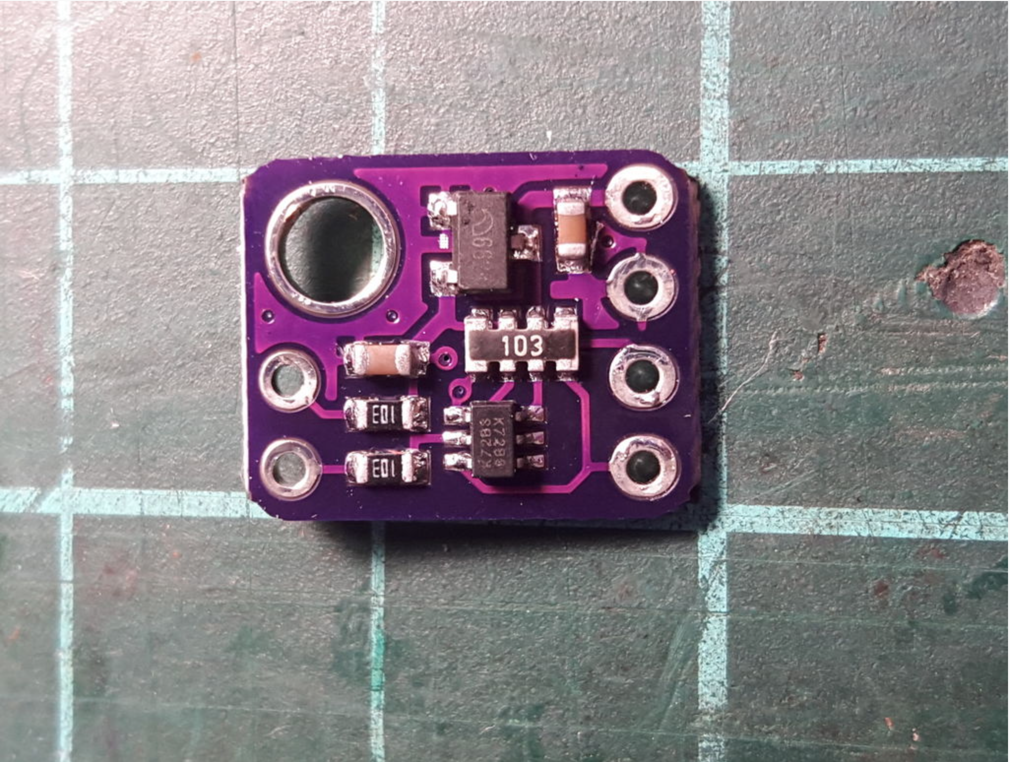
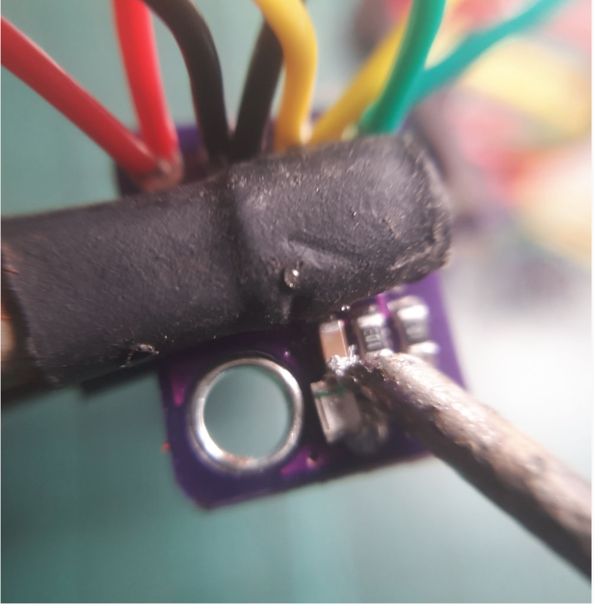
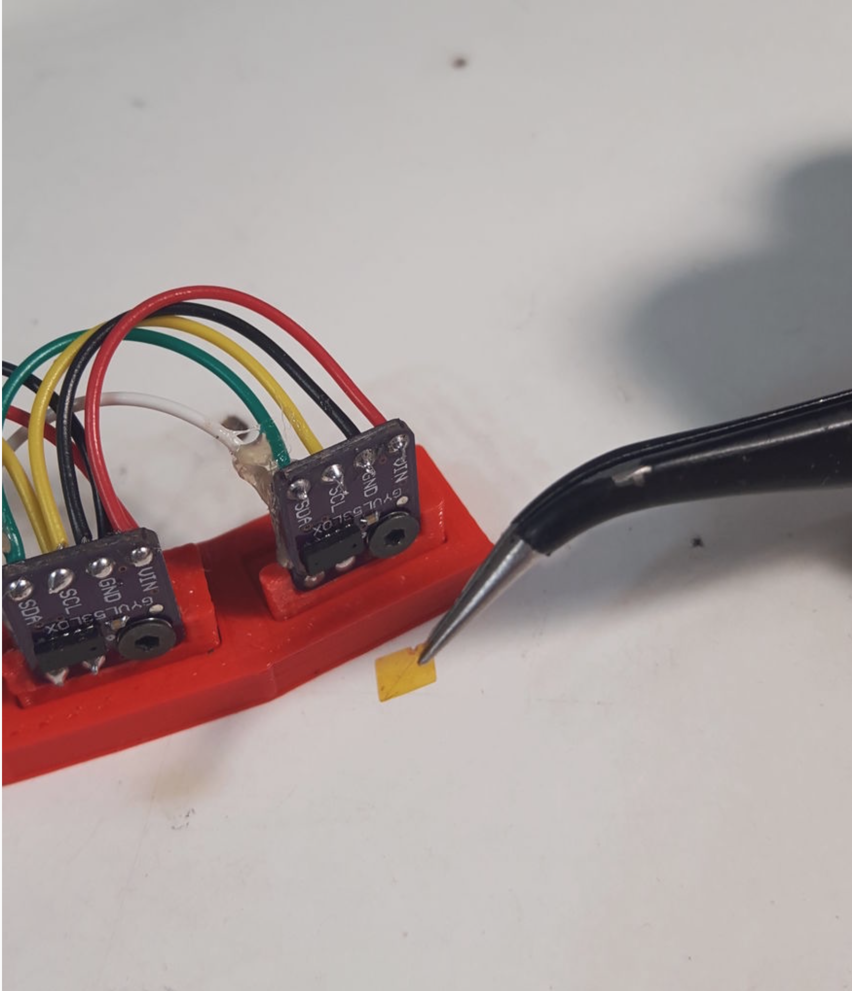
Adding a LED
In the next step, a small 0805 SMD LED will be added to the breakout board, connected from the XSHUT pad to the GND terminal of an adjacent capacitor. Although LED itself does not affect the operation of the module, it does give us a good visual indication on the XSHUT logic level.
Hooking the LED in series with the pull-up resistor (10k in my case) on the XSHUT pin will introduce a voltage drop. Instead of high logic level of 3.3v, the forward voltage drop for a red 0805 LED is measured 1.6v. Although this voltage is higher than the high logic level (1.12v) in datasheet, blue LED is better for this hack. The forward voltage drop for blue LED is measured about 2.4v, which is safely above the chip's logic level.
Adding the N-MOS Inverter (Logic NOT Gate)
A small SOT-23 N-channel MOSFET is stacked on the LED we have added. Two terminals (D, S) need to be soldered on the breakout board, and the remaining terminal (G) is connected to the upstream board GPIO pin using #26 wire.
Notes on Adding SMD Components
Soldering SMD components on a breakout board not designed for, is not a easy task. If you haven't heard of 0805, SMD, SOT-23 yet, the chances are that you haven't solder those tiny little components before. While handling those tiny components by hand, it is very common that:
- The little thing just dropped off and disappeared, forever,
- The tiny pads on the little thing just peeled off.
- The tiny legs on the little thing just broke.
- The soldering tin just gathered into a blob and couldn't be separated.
- And more...
If you still want to make this radar, you can:
- Change the components to larger package, such as DIP style.
- Get more components than minimum required, for practice and consumption.
Soldering the 0805 SMD LED
Soldering a 0805 LED by hand, on a breakout board not designed for SMD, is not an easy task at all. The following steps is my recommendation to solder the LED.
- Use the helper hand to hold your breakout board.
- Put some soldering paste on the edge of the SMD capacitor and the "XSHUT" pad.
- Use the soldering iron to put some additional solder on the capacitor edge.
- Put some soldering paste on both ends of the 0805 LED.
- Use the soldering iron to put some tin on both ends of the 0805 LED.
- Use the tweezers to place the LED as shown in the photo.The cathode end normally has a marked line. In my example, there is a green line on the cathode end. Place the cathode end to the capacitor end.
- Use the tweezers to add light pressure on the LED towards the capacitor, and solder the LED to the capacitor end, by adding heat to the capacitor end at the same time. Do not press to hard on the LED. Its cover may break under heat and excessive pressure. After soldering, add gentle pressure on the LED sideways, to test if the LED is soldered in place.
- Now solder the LED at the XSHUT dip pad. This step should be easier.
Note: The capacitor end shown in the picture is the ground terminal on this breakout board. And the dip pad XSHUT is pulled-up by a resistor.
Testing the LED
The LED should light up when you apply power (e.x. 5V) and ground to the breakout board.
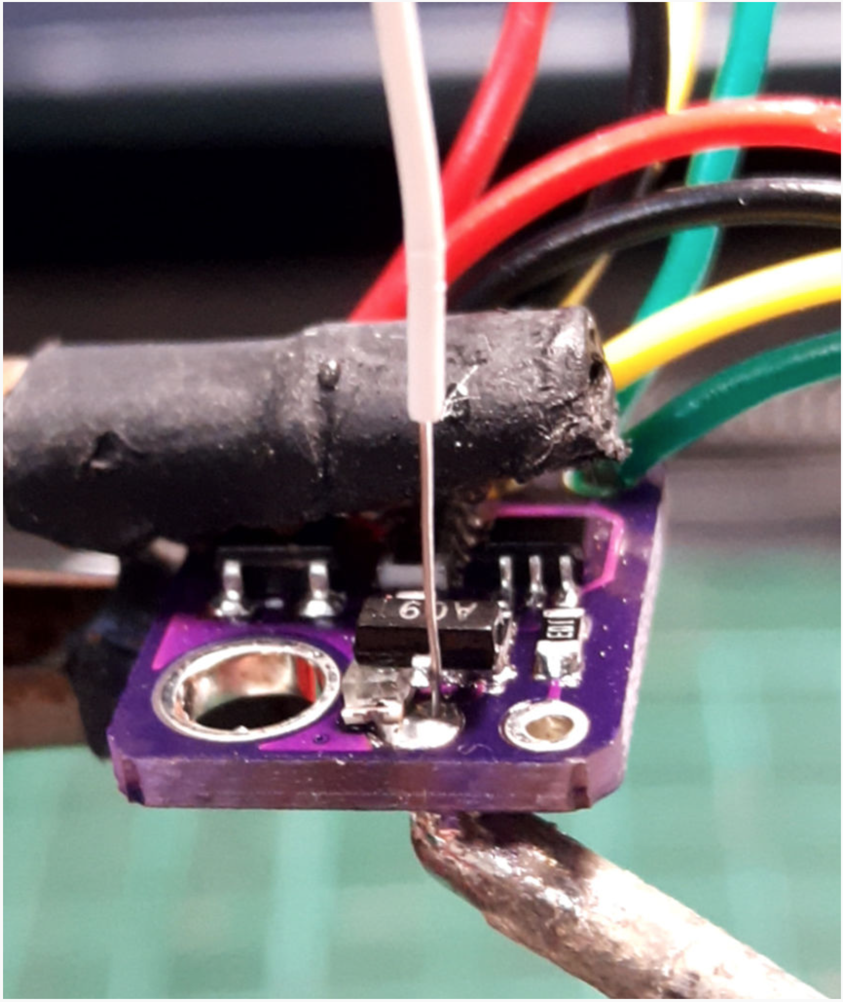
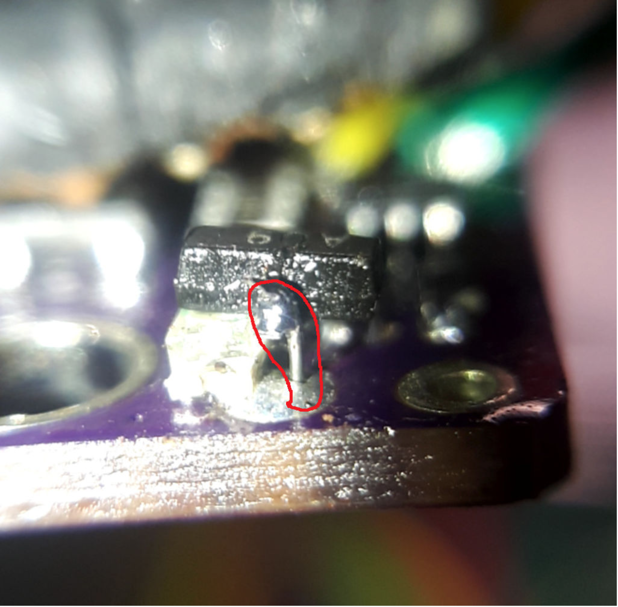

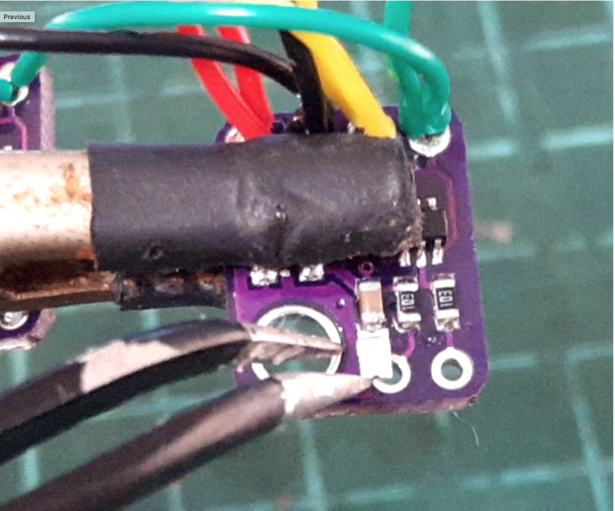
Soldering the AO3400 N-Channel MOSFET
This MOSFET is in SOT-23 package. We need to "stack" it on the LED, and add a wire as well:
- Put some soldering paste and tin all three terminals.
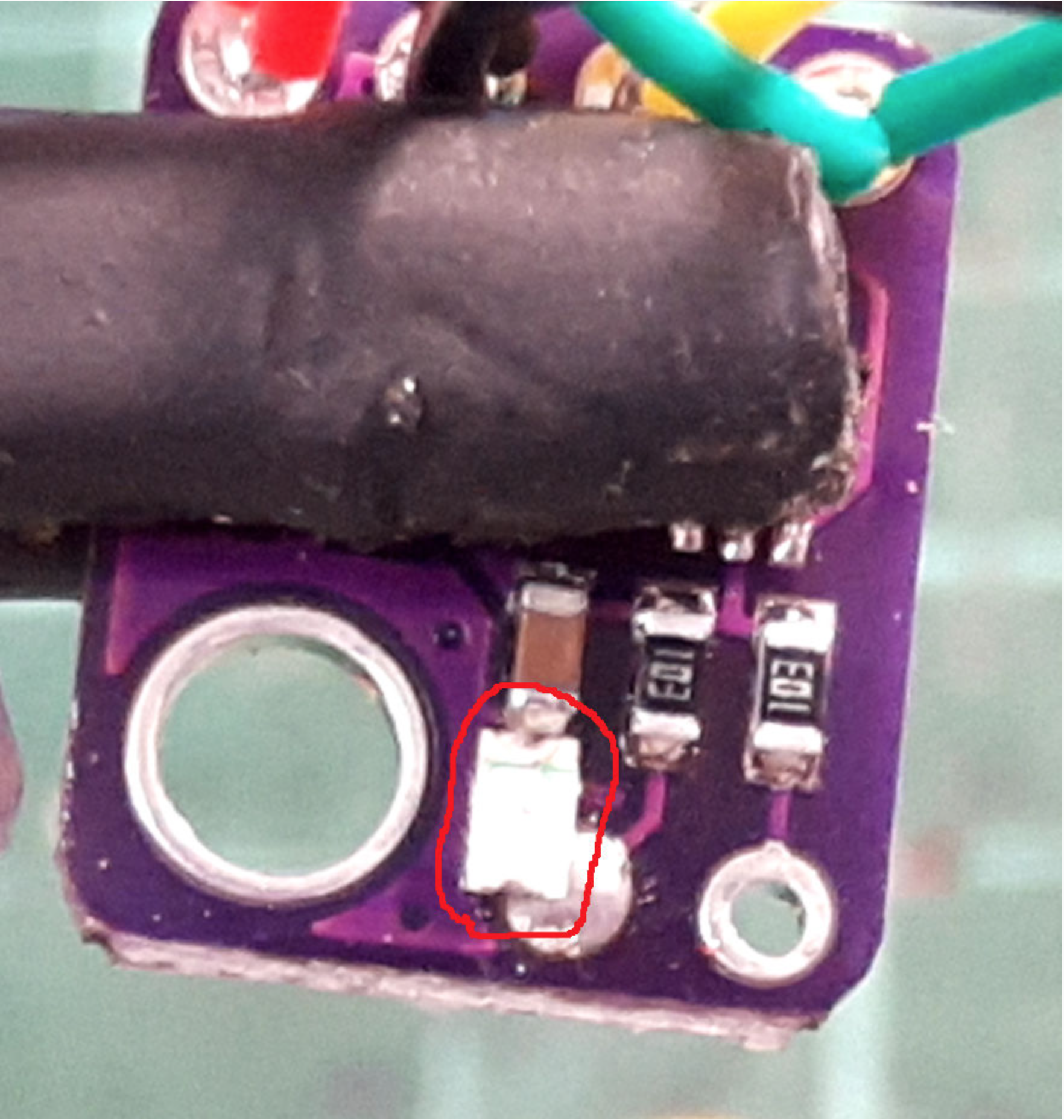
- Use tweezers to place the MOSFET on top of the 0805 LED. The S terminal should touch the top of the capacitor
- Solder the S terminal with the capacitor end, as shown in the photo.
- Cut a small section AWG #30 single core wire, and remove the coating about 1cm.
- Use the soldering iron to melt the solder in the XSHUT hole from below, and insert the #30 wire from above, as shown in the photo.
- Soldering the upper end of the wire to the MOSFET D terminal.
- Cut off extra wire.
Note: The MOSFET S terminal is connected to the capacitor end as shown in the picture. This end is the ground terminal. The MOSFET D terminal is connected to the original XSHUT pin.
Terminal G is not connected at this moment. Its position is just above some pull-up resistors. Make sure there is a gap between them (N-MOS and resistor) and does not contact with each other.
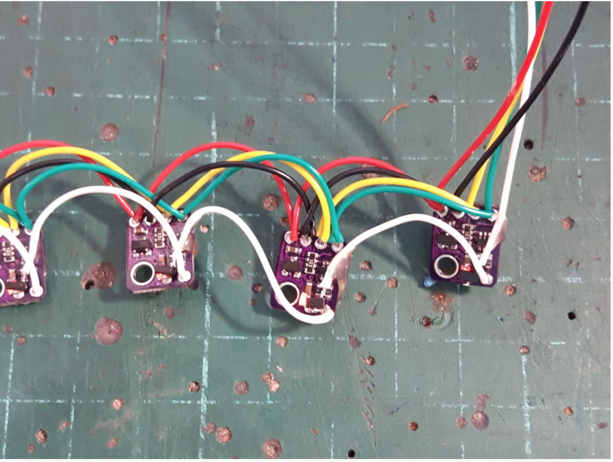
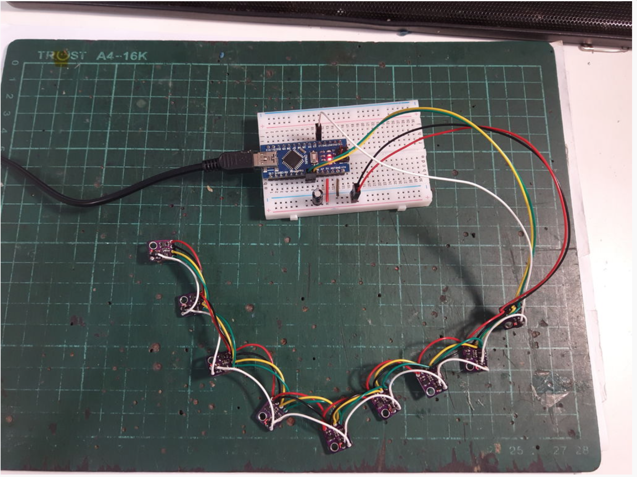
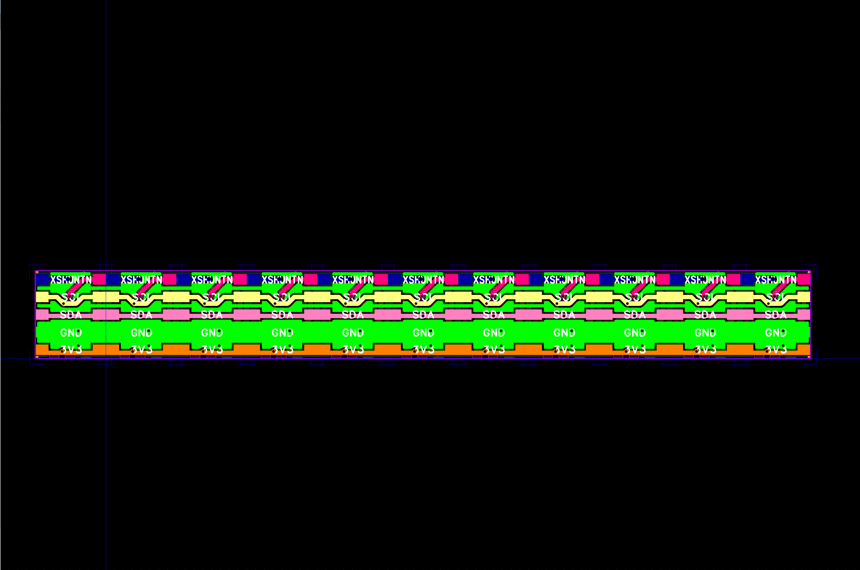
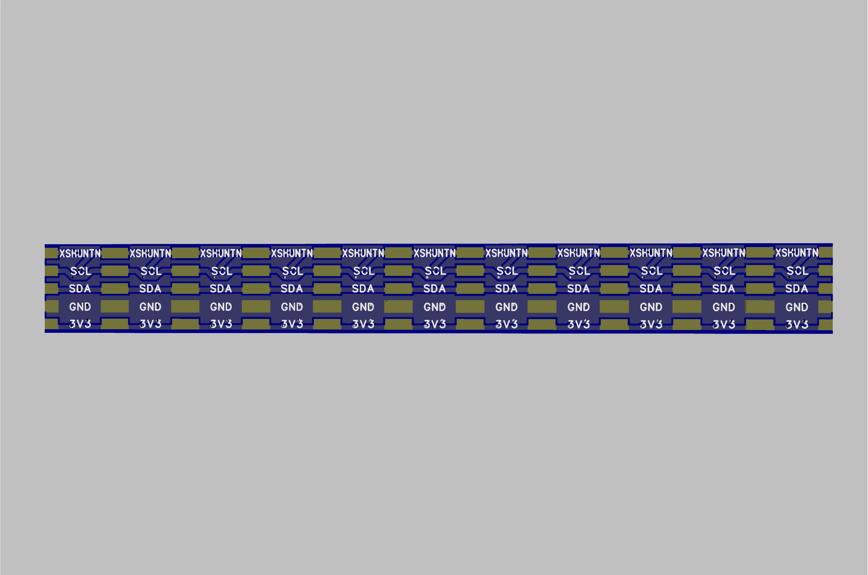
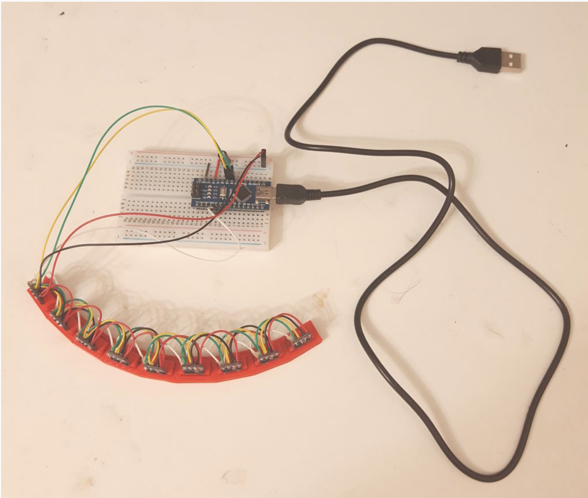
Common Bus Wiring
Common bus includes:
- Vcc power. Red in photo. I am using arduino nano with 5v logic. The breakout board has LDO and level-shifter. So it is safe to use 5v as Vin.
- Ground. Black in photo.
- SDA. Green in photo.
- SCL. Yellow in photo.
These four lines are common lines. Cut appropriate length of wires and soldering them in parallel, to all sensor modules. I used 20 cm from arduino to the first sensor, and 5 cm each thereafter.
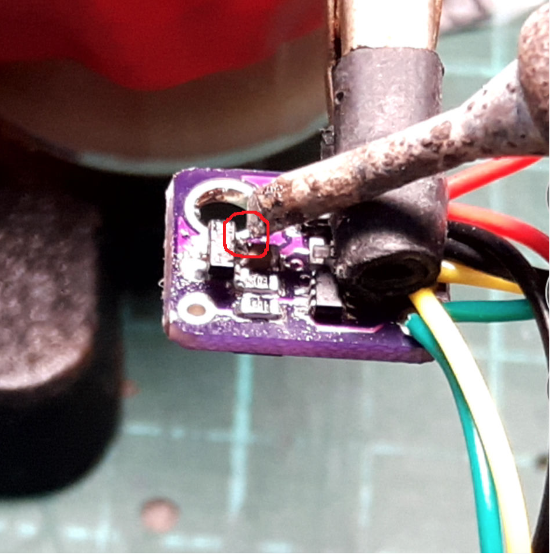
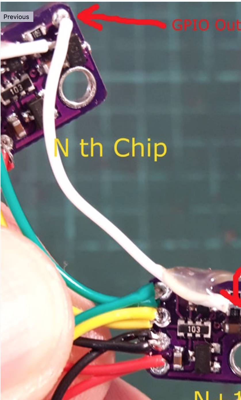
XSHUTN and GPIO Wiring
The 20 cm white wire is from arduino control pin, to the XSHUTN pin of the first sensor. This is the control line required to bring the first VL53L0X chip out of reset and change the I2C address.
The 5 cm white wire between each module is the daisy chain control line. The upstream chip (for example, chip #3) GPIO pad, is connected to the downstream (for example, chip #4) XSHUTN leg (N-Channel MOSFET G terminal).
Be careful not to make the G terminal contact with the resistor below. You may add a insulation tape in the gap. The protection liner usually supplied with the VL53L0X chip can be used here.
Use the heat gun to stick the control wire.
Hot Glue
As you can see in the photo, there is a blob of hot glue on the white control wire, near the N-MOS G terminal. This step is very important and absolutely necessary. A floating soldering directly to the SMD component's leg is very weak. Even a small pressure on the wire may break the leg. Do this step gently.
Testing the LED
When you apply power (ex. 3.3v-5v) and ground to the sensor array, the LED on the first module should respond with the XSHUTN wire logic level. If you connect the XSHUTN to logic high (ex. 3.3v-5v), the LED should be off. If you connect the XSHUTN wire to low (ground), the LED on the first module should be on.
For all subsequent modules, the LED should be off.
This test is conducted before connecting to the arduino.
Daisy Chain Testing
Now we want test if the I2C address change works for all the sensors in the array. As mentioned, the first chip is controlled by the arduino. The second chip is controlled by the first chip, and so on.
- Setup the bread board. 5V and Ground rail are directly connected from adriano 5V and ground. Current consumption for each sensor is rated 19ma in datasheet.
- Add a capacitor on the power rail to help stabilizing the Vin.
- Connect Vin and Ground from the sensor array to the power rail.
- Connect SDA to arduino Nano pin A4 (may be different for other micro-controllers).
- Connect SCL to arduino Nano pin A5 (may be different for other micro-controllers).
- Connect the XSHUTN wire to arduino Nano pin D2. (This can be changed in sketch).
- Go to github https://github.com/FuzzyNoodle/Fuzzy-Radar and download the library.
- Open the "Daisy_Chain_Testing" example and upload the sketch.
If everything works, you should see the status LEDs light up one by one, similar to the video clip above.
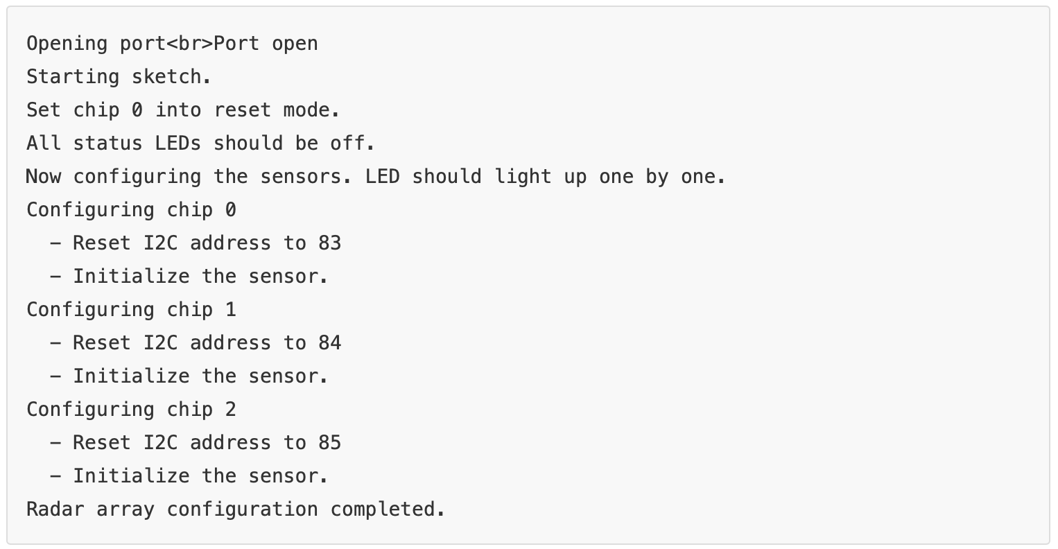
You may also open the Serial Window, and see the initialization progress. The output would appear like this:
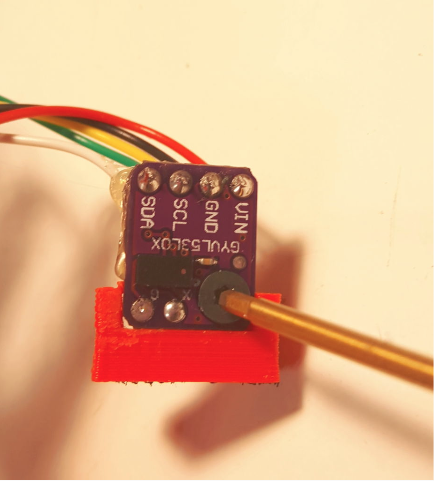
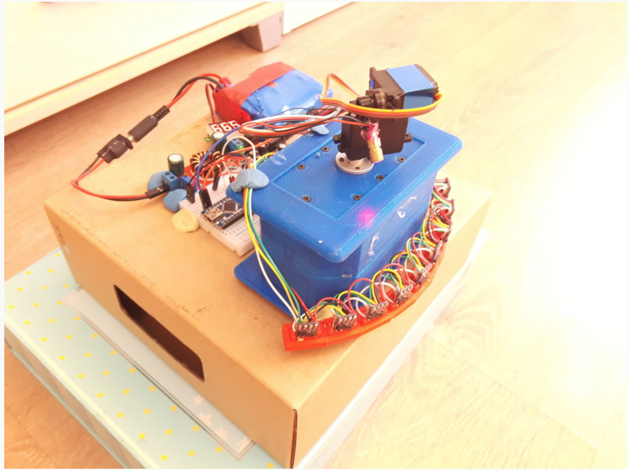
Assemble the Holder and Frame
- Carefully place each GY-530 module on the holder with the M2x10 screw. Do not press the MOSFET or pull the XSHUTN wires.
- Place each holder into the circular frame. Use some hot glue to bond the parts.
Again, the M2 screws, holders and circular frame are used to place the sensors in a circular arrangement. You may use any other methods, such as using card boards, model woods, clay, or even hot glue them on a can.
The 3D printed files I used are provided below. The circular frame has 9 modules, and separated by 10 degrees each. If you have a sharp eye, there were 10 modules in previous photos. The reason? Explained below...
Remove the Protective Liner
If you followed the steps from the beginning, it is a good time now to remove the protective liner on the VL53L0X chip. On my previous photos, they are already removed because I have to test the modules and make sure the concept works before posting this instructables.
About the protective liner, datasheet states: "It must be removed by the customer just before mounting the cover glass". The two tiny holes (emitter and receiver) on the VL53L0X chip are vulnerable to pollution, such as dust, grease, hot glue, etc...
Once polluted, the range may be reduced, and the readings may be off by an obvious amount. One of my test module is accidentally polluted by glue clay, range is reduced to 40cm, and the distance reading is erroneously enlarged by 50%. So, be careful!
*.stl files for 3D printed parts used in this project can be downloaded in the files section.
Using the Raw_Data_Serial_Output example
Now we really like to see the data from our sensor array. In the arduino library on GitHub:
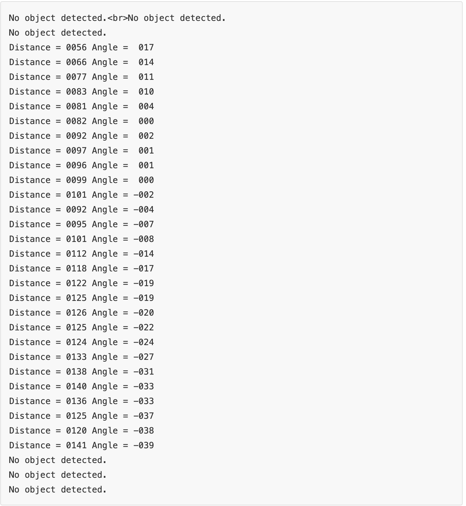
There is an example called Raw_Data_Serial_Output. This example demonstrates the raw data output from the sensor array. The output values are in millimeters.
After the sensors are initialized, should see something like this in the serial window when you wave your hand through the sensors:
Refer to the video clip for a live demonstration.
Using the Fuzzy_Radar_Serial_Output example
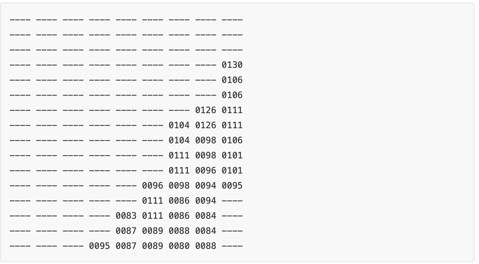
The next step is to get useful data out of these distance readings. What we wanted from a RADAR are the target object's distance and angle.
- The distance is in millimeters, related to the sensor surface. Returning 0 means the the target is out of range.
- The angle is in degrees, on the horizontal plane. The code currently expected the sensors are spaced evenly. Returning 0 degrees means the target is at the center position of the array.
Some filtering algorithm are applied in the library:
- Noise removal:
- Short (in terms of sample count) readings are considered noise and are removed.
- Readings that are far away from mean value are removed.
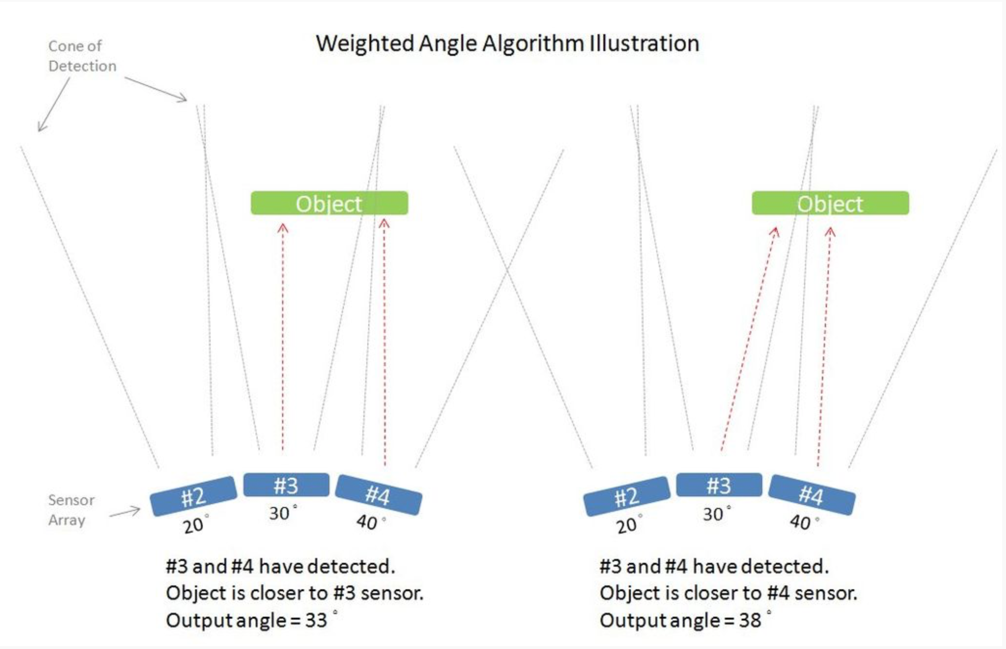
- Weight angle calculation (see illustration above)
- Target object is assumed to be a flat surface
- If multiple sensors have detected the object at the same time, a weight is calculated for each sensor.
- The weight for each sensor is inversely related to its distance.
- The result angel is calculated from weighted angle of each sensor.
- Primary target selection:
- If there are more than one group of readings, the widest (with more sensor reading count) group remains.
- For example, if you put two hands in front of the sensor array, the hand detected by more sensors remains.
- Closest target selection:
- If there are more than one detected group with same width, the group in closest distance remains.
- For example, if you put two hands in front of the sensor array, and two detected groups have the same sensor count, the group closer to the sensor remains.
- Output distance and angle are smoothed through low pass filter.
In the Raw_Data_Serial_Output, the raw distance readings are converted into distance and angle value. Once you uploaded the sketch, you may open the serial window to see the result similar to this:
So now, you have a RADAR (LIDAR):
- Smaller than ultrasonic sensor modules
- No moving parts
- Scans at 40 Hz.
- Shaped like a belt, can be mounted on a circular frame
- Use only three control wires, plus power and ground.
- Has a range from 30 millimeters to around 1000 millimeters.
In the following steps, we will show you some cool demonstrations!
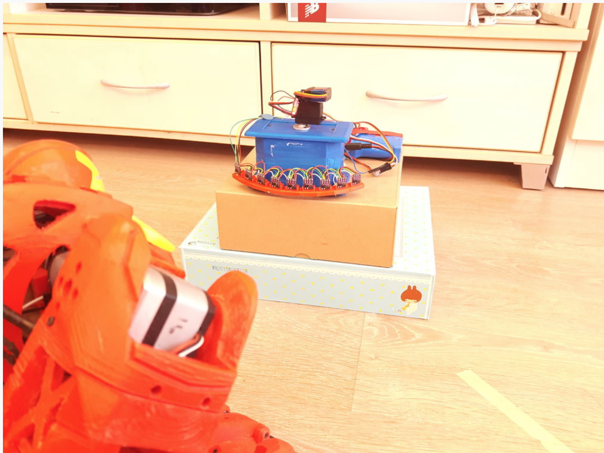
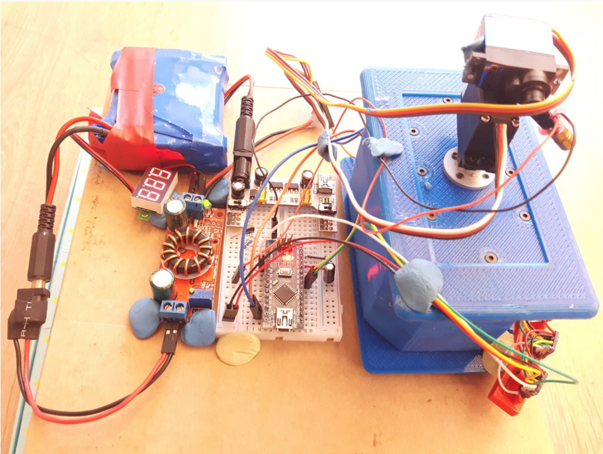
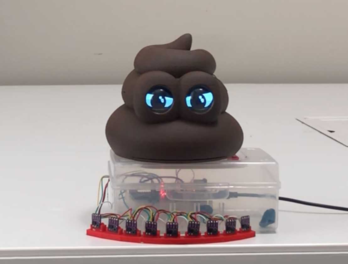
This is one example of using the Stationary Radar we have built from previous steps. This step is not written in detail, as this is a demonstrator of the Radar. In general, you need these additional items to built this demonstration project:
- Two servos
- A laser pen emitting head
- A MOSFET or NPN Transistor to control the laser head output
- A power source for the servos. It should be separated from the micro-controller.
The code can be downloaded here.
Please see the video provided.
Demonstration of using radar away to track object location and distance.
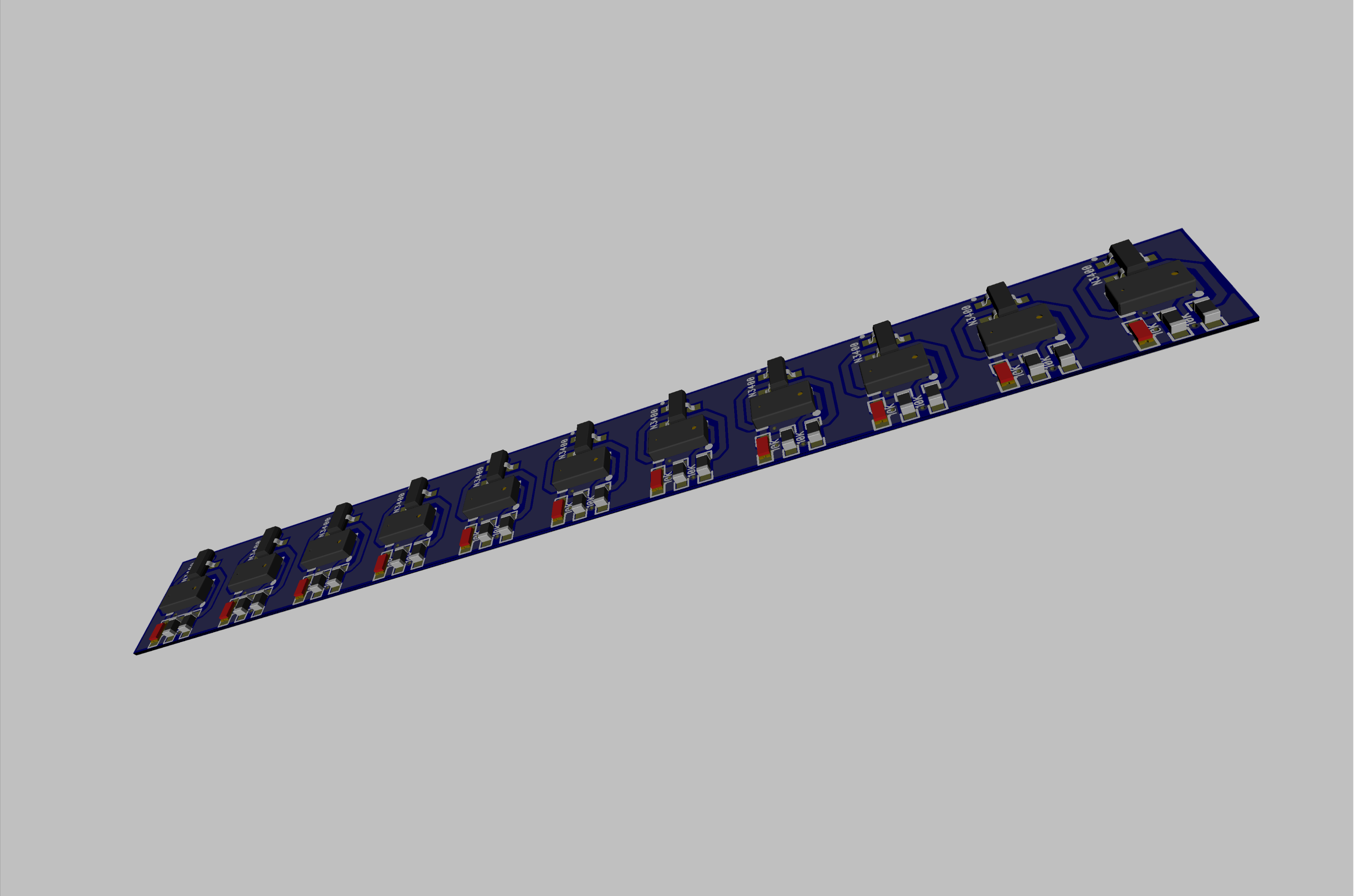
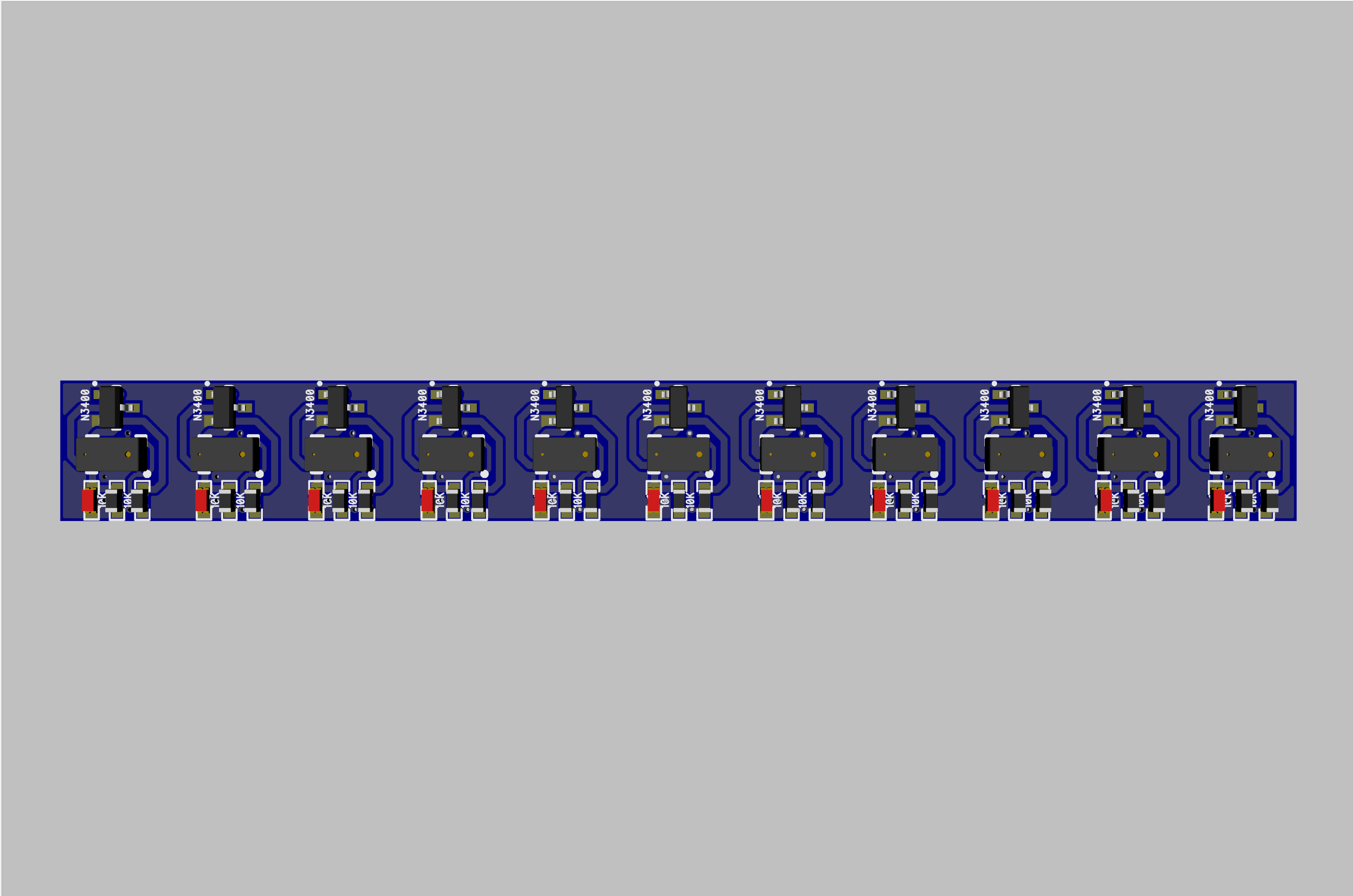
Schematic and Gerber files for PCB can be downloaded in the files section of this project.