 dsl
dslIntroduction
I'm going to include a review for PCBWay service as a part of this update because they supported me with the current iteration of Xling v3.2 and manufactured black PCBs for free.
However, I'd like to keep it as fair as possible because everyone should benefit in this case. On one hand, everyone who's reading it will be able to understand what PCBWay is capable of. On the other hand, PCBWay will be able to see what they might improve in their service.
Personally, I'd like to thank DI HALT and his blog, easyelectronics.ru. I read it from time to time with pleasure. Besides, an article about PCBWay helped me a lot.
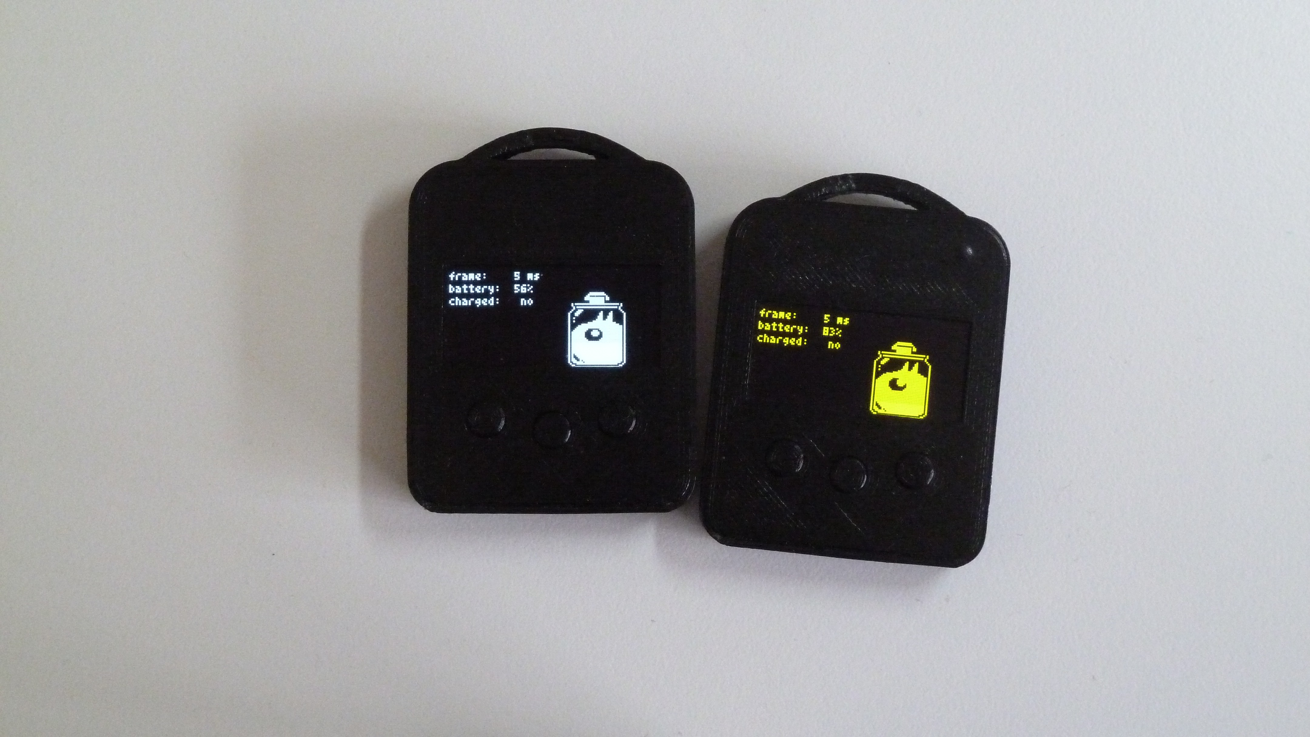
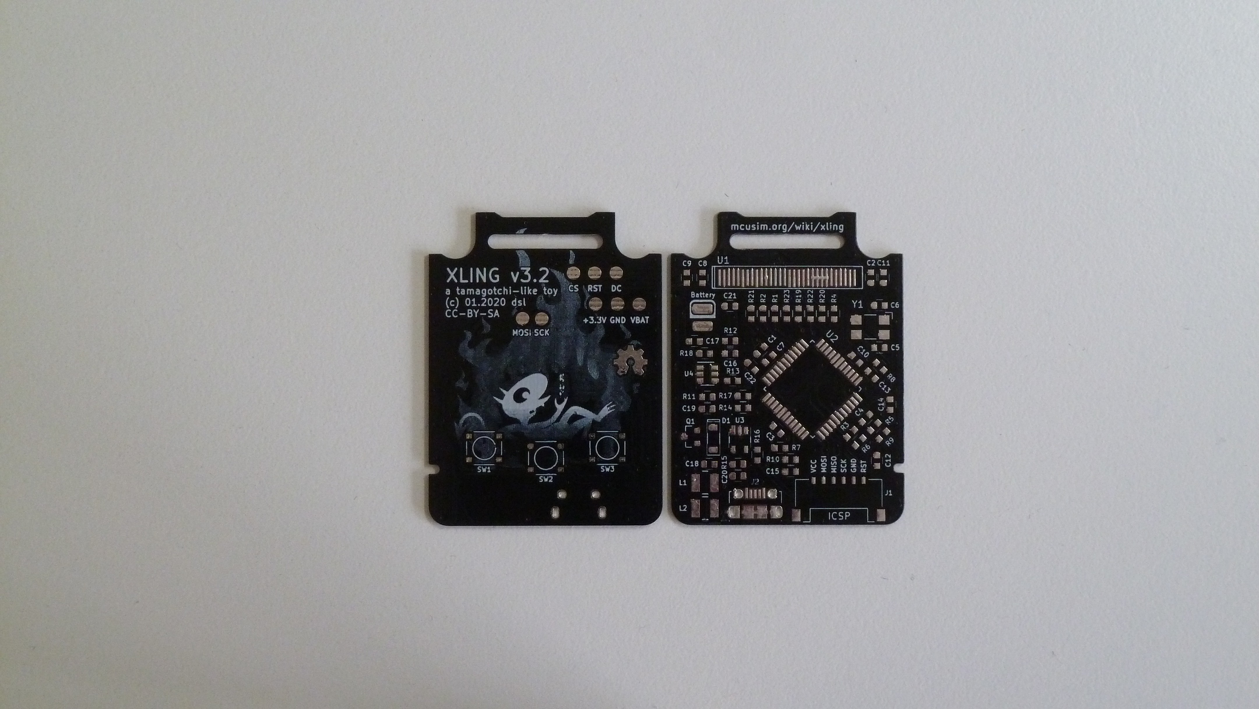
Let me show you how Xling looks like in its current iteration fully assembled and in a 3D-printed case.
Just as I imagined!
How to configure PCB
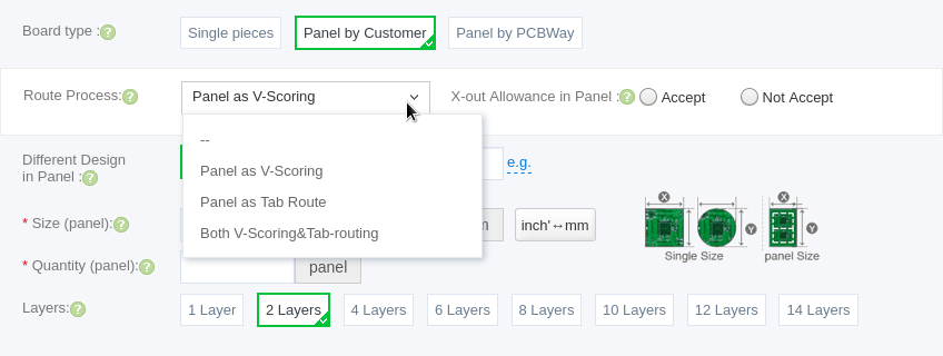
Board type parameter means a way to prepare PCBs. You'll receive boards in single pieces in case of the first option which is suitable for prototypes or a small batch production. The second and third options which start with Panel by... might be useful in case of an automatic assembling and a mass production and allow you to select your own size of a panel (Panel by Customer) and let PCBWay populate it with your boards, or let PCBWay to do all of these steps (Panel by PCBWay).
Please, note that in case of a single board it's necessary to select Size of a single board only, but in case of a panel, these are dimensions of the whole panel which might contain several boards. The same rules are applicable for Quantity which means a number of single boards or a number of panels accordingly.
Generally speaking, it's not obvious why somebody would let PCBWay to decide how to panel her boards because dimensions of a panel depend on a specific assembly equipment. However, PCBWay offers an assembly service also and the third option is useful in this specific case.
There are several ways how boards will be connected within a panel. In case of V-Scoring PCB material will be cut for a half of its height to simplify a break off. In case of Tab Route boards will be attached to a panel and among each other by narrow bridges.
It might also be necessary to include different designs into a single panel, but it'll increase its price.
Another option called X-out Allowance in Panel gives an incredible ability to reduce an overall cost of the panel by about 30%. It's useful if you can tolerate a PCB in the panel to fail electrical testing. It'll be marked by a cross in this case.
You shouldn't usually worry about number of Layers because it can be obtained automatically from Gerber files provided within an archive.
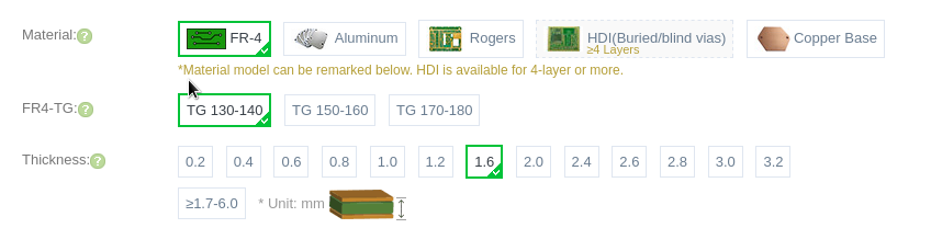
Material is what PCB is manufactured from, where FR-4 is epoxy glass cloth (the most widely used material for PCB, probably) and the rest.
Personally, I'd like to mention FR4-TG which stands for a glass transition temperature and defines some thermal and chemical properties of the material. One of the most important things which is affected by this temperature is board geometry which is critical in case of really narrow routes and precision PCBs. The higher the temperature, the better PCBs can be manufactured, but overall cost will be increased also.
Another important option is HDI (Buried/blind vias) which stands for High Density Interconnect PCBs. In this case RCC (Resin Coated Copper) is applied to epoxy glass cloth which leads to fine circuits.
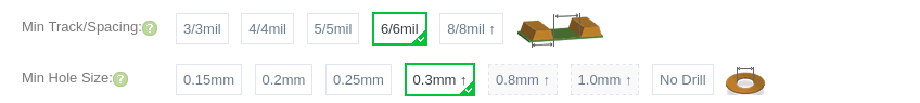
These are limits for tracks/spaces and size of the holes. Please, be careful and select them according to your design.
It's interesting how minimal these options are. For example, you cannot select a limit for annular ring, but a diameter only. Personally, I'd recommend to read about PCBWay capabilities first in order to stay within limits and reduce amount of money to be spent on PCB production.
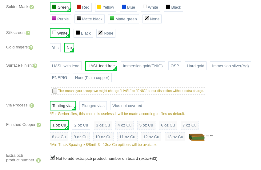
There is a plenty of Solder Mask colors available, but unusual ones might affect an overall price of the PCBs. This is especially true and a subject to double check in case of Matte black and Matte green options.
Gold fingers are useful when there are contact pads on a side of your board (like on various PCI cards in your PC). This option helps to tell PCBWay to cover only these pads with immersion gold (ENIG) instead of the whole PCB copper. Another way to reduce costs.
Be careful with the material for gold fingers! It's a "hard gold" by default which could easily lead you to bankruptcy.
I'd like to stop at Surface Finish options and explain them in details. There are several ways to process copper layers in order to satisfy soldering requirements (plain surface is usually necessary for fine pitch ICs, for example) and/or protect copper from environment.
HASL, which stands for Hot Air Solder Leveling, is a cheap and affordable option which can also be used to repair your prototypes, i.e. it's easily re-solderable. It comes in two flavours with lead (a chemical element with the symbol Pb) and without.
I strongly recommend you to use only lead-free HASL for all of your prototypes in order to avoid potential harm for humans and nature. Please, remember that lead is a highly poisonous metal, affecting almost every organ and system in the human body.
OSP, which stands for Organic Solderability Preservative, is some kind of a varnish for copper layers which protects it. OSP makes copper flat enough and allows you to use almost any solder (lead and lead-free). However, it can be damaged easily which makes it a poor choice if you're going to store your PCBs for any significant amount of time, e.g. more then several months.
ENIG, which stands for Electroless Nickel/Immersion Gold, is some kind of a "pie" where copper layers are covered by nickel, and nickel itself is protected by gold. A perfectly flat surface is the result of such process which doesn't have shortcomings of the OSP. However, a "black-pad" could form during the electroless nickel plating step which reduces solder joints reliability. Anyway, ENIG might be necessary if you've large BGA packages on your boards. And it usually increases costs.
ENIG might look like an expensive option for the first sight, but price per PCB can be significantly reduced by ordering even a small batch of, say, 50 pieces.
For example, 5 single pieces of Xling v3.2 cost me $66 (including DHL delivery) with ENIG surface finish which means that I pay $66 / 5 = $13.2 per PCB. However, 50 single pieces of Xling v.3.2 cost me $85 (including DHL delivery) which means that I pay $85 / 50 = $1.7 per PCB.
Almost 8 times less!
Immersion silver (Ag) combines the advantages of ENIG and HASL, but might suffer from rapid surface degradation because of oxidation. And, of course, it's expensive even for 50 pieces batch.
Via Process shouldn't usually be tweaked at all because a required value will be obtained from your Gerber files from an archive.
There is a nice additional option available which allows you to remove any production marks from your PCB, but it costs $3 extra.
This configuration has been used to prototype Xling v3.2:
Board type: Single PCB
Size: 35 x 47 mm
Material: FR-4
FR4-TG: TG 130-140
Thickness: 1 mm
Solder Mask: Black
Surface Finish: HASL lead free
Layers: 2 layers
Min Track/Spacing: 6/6mil
Silkscreen: White
Additional Options: Extra PCB product number removed
If you're going to panel your PCBs, it might also be necessary to have a stencil.
How to configure SMD stencil
SMD stencil is particularly useful in a stencil printing process which allows you automatically populate solder paste to pads on a board.
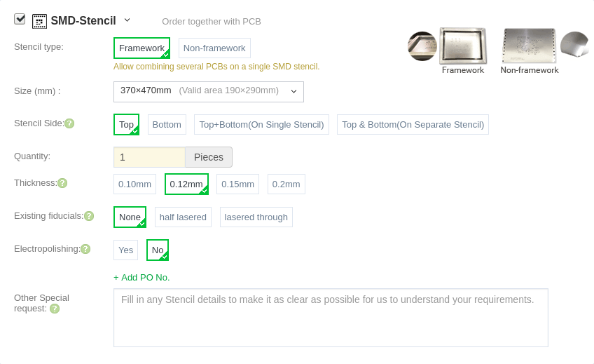 Let's take a closer look at the available parameters.
Stencil type means a way to prepare a stencil (with frame or without). It depends on your assembly equipment.
Size of a stencil can't be smaller than a panel itself, but can easily be bigger. It also depends on the assembly equipment.
Be careful with a "single board" type (or incorrect panel size) and SMD stencil. You might be lucky enough to receive a huge sheet of metal with a little stencil for a single board cut at the center.
It might be necessary to have stencil for top and/or bottom side of a PCB or a combination of them. Stencil Side parameter helps here.
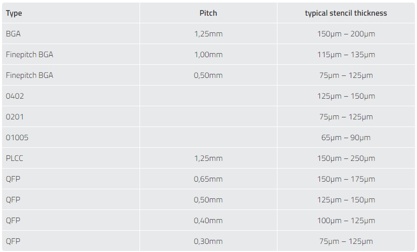
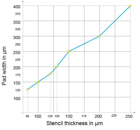
Thickness of a PCB stencil allows you to choose how much solder paste will be left on pads. This parameter is defined by a smallest pad on the PCB.
Thanks to DI HALT, we've a table and a diagram to select a correct thickness.
Existing fiducials are some kind of markers on a stencil to place it on a panel correctly. They can be engraved (half lasered) or cut through (lasered through).
Electropolishing helps to avoid sharp edges (which might remove a small, but significant amount of solder paste from tiny pads) after laser cutting. It makes sense for anything smaller than 0805.
Production time
It took about three days from my order posted to its shipping. So, in this case service was exceptionally fast.
A closer look to PCB
This is how boards look like without a microscope:
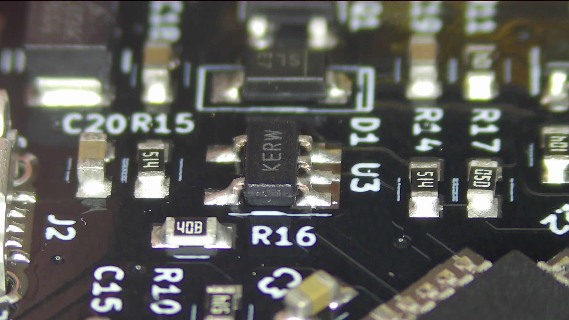
Everything seems fine for the first sight. Even a silkscreen picture looks really good to me. Let's take a closer look:
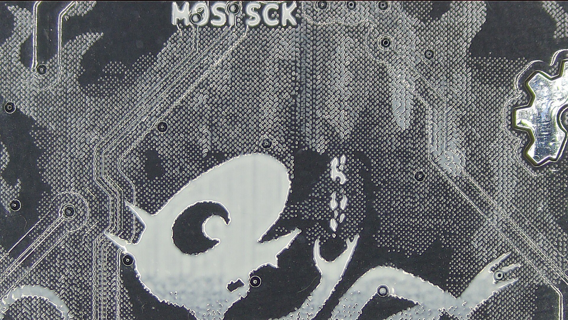
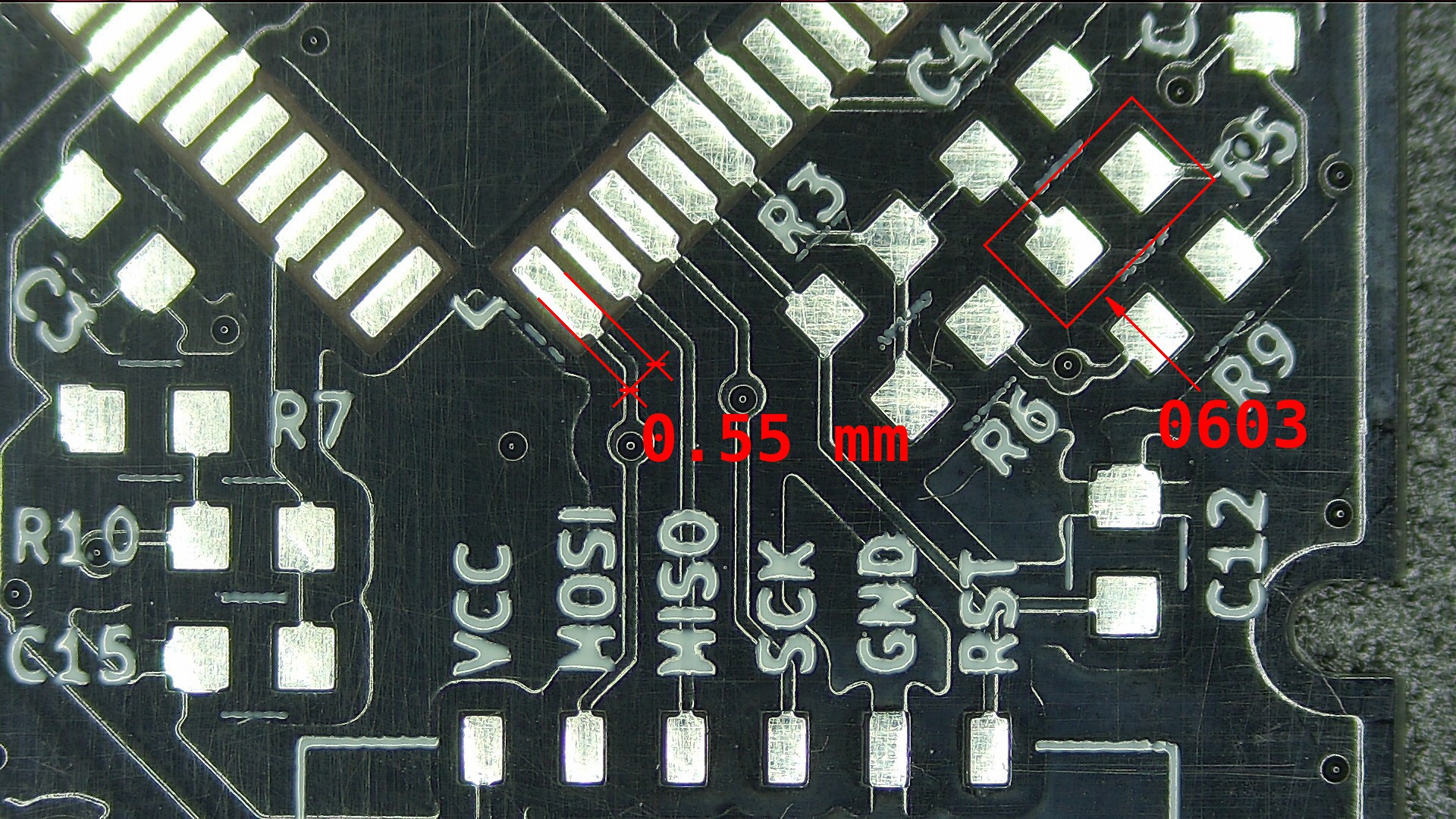
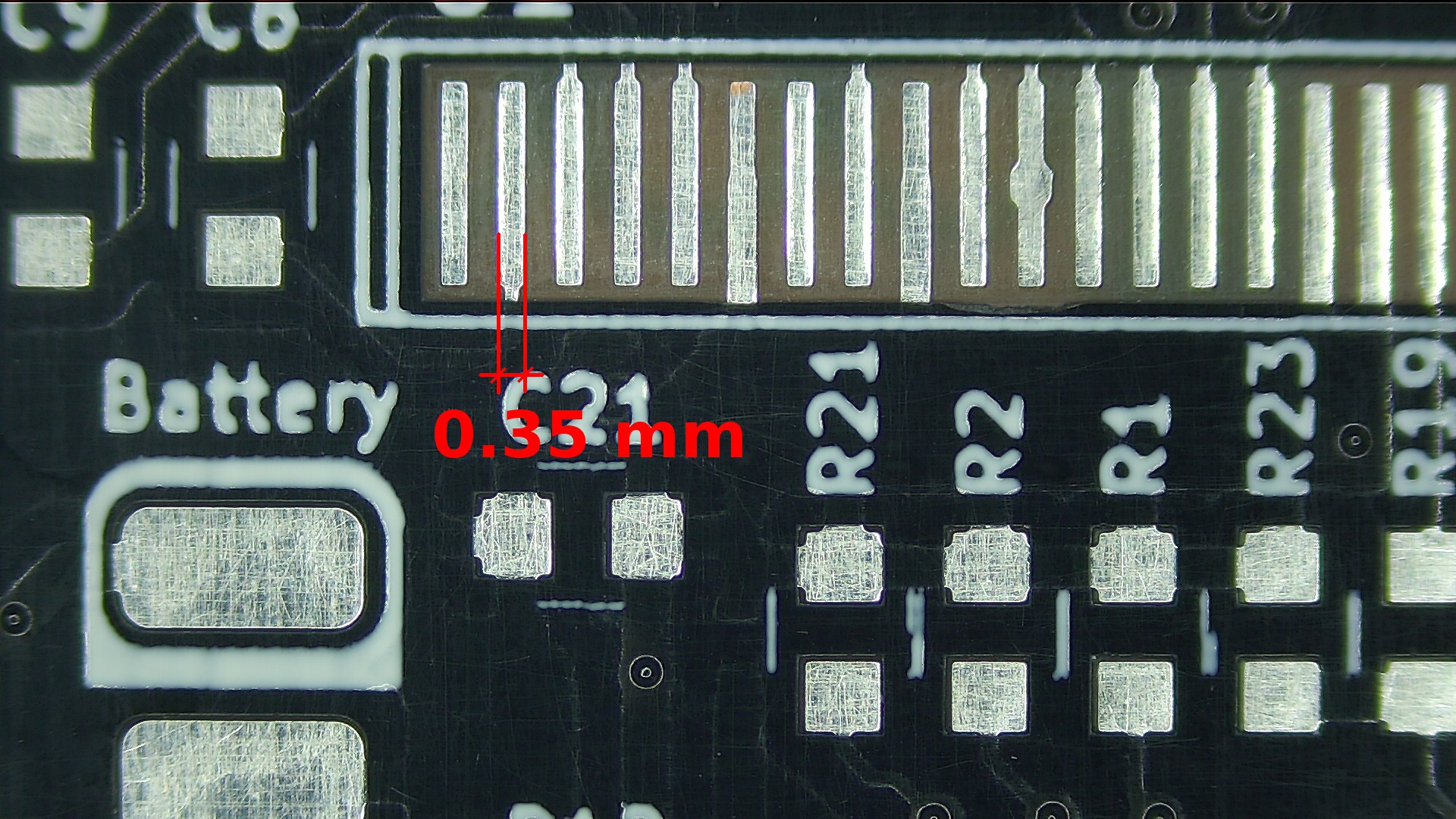 All of the pads seem fine. Even the smallest ones for OLED flat flexible connector look good to me. There are minor issues with silkscreen, but it could be my mistake during PCB design. All of the labels are readable.
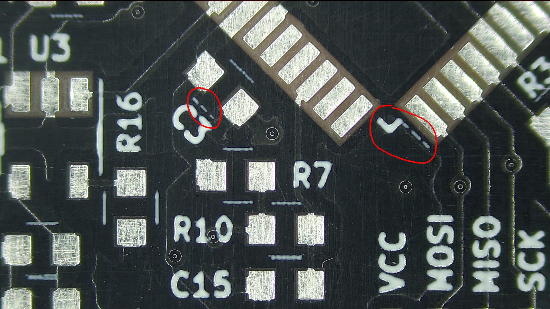
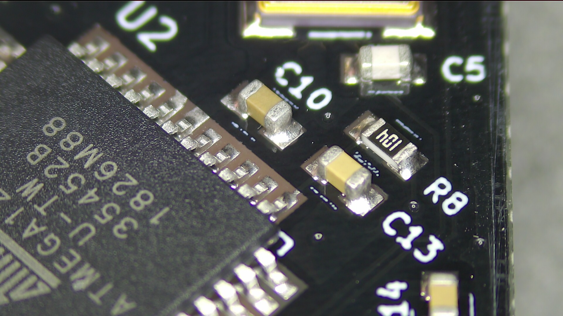
I spent some time assembling a prototype: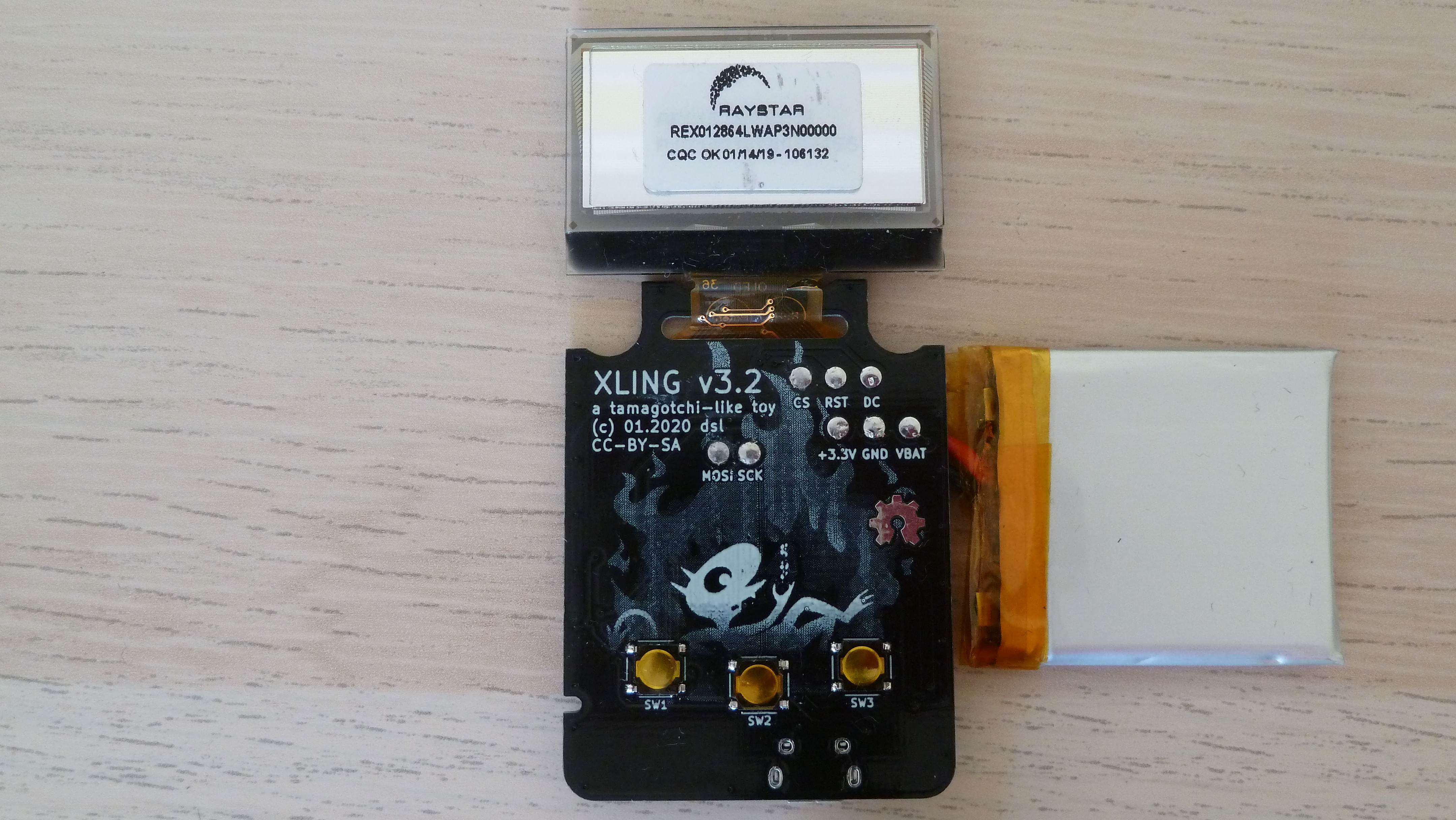
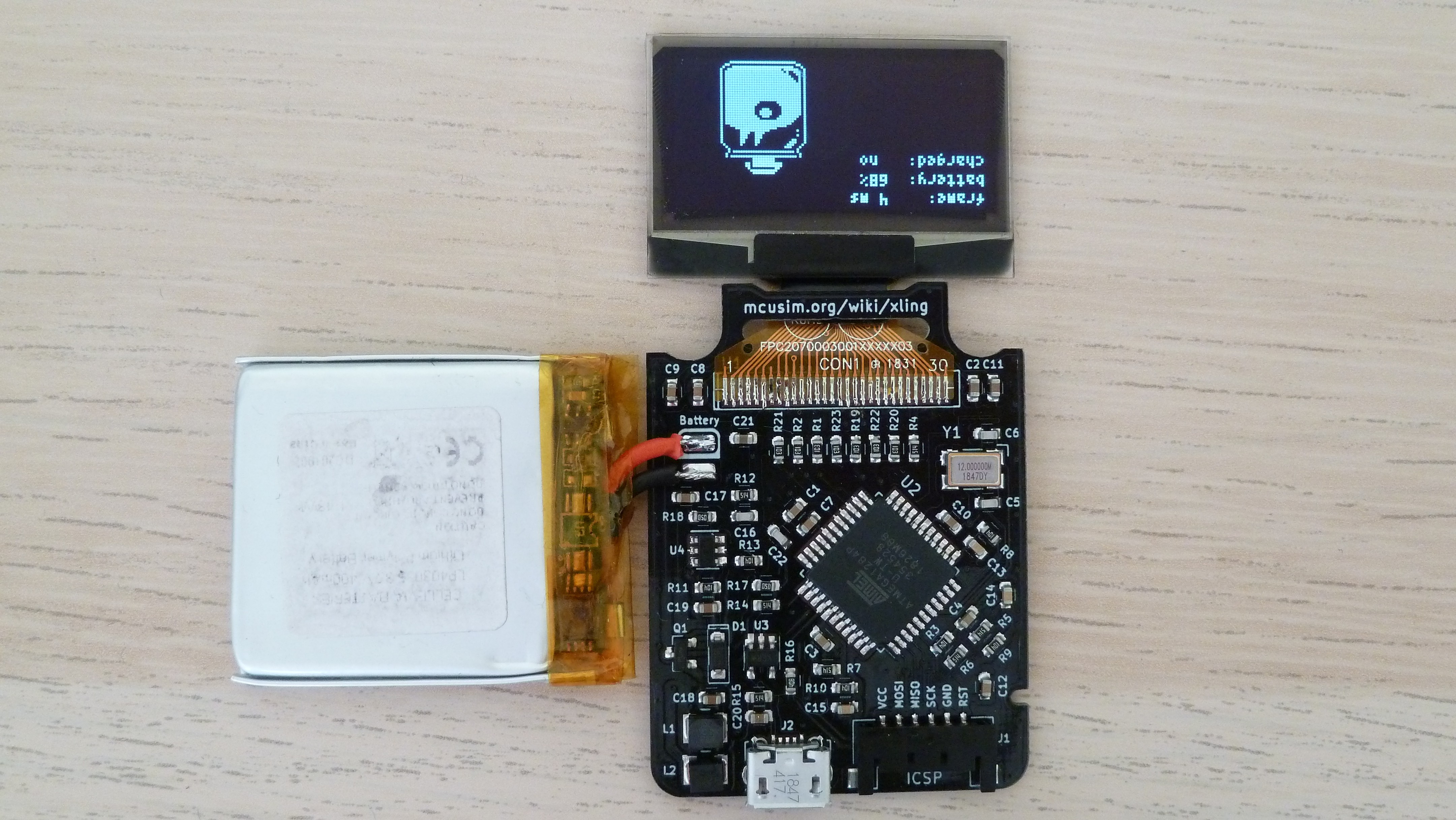 There were no issues during components placement and soldering with hot air gun and a soldering iron itself.
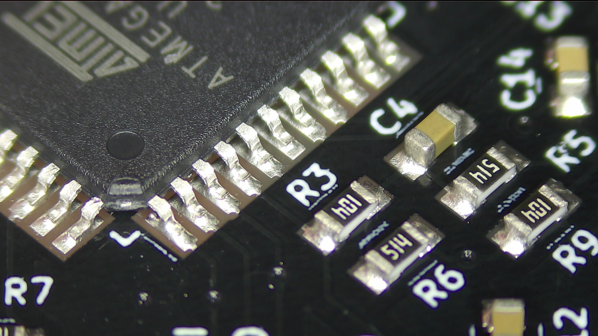
This is how assembled PCB looks under microscope:
Firmware bugs fixed
I'd like to mention a specific commit in the Xling repository which helps to fix device hanging on a way from/to sleep mode.
To sum it up, I got rid of the direct control functions to manipulate the FreeRTOS tasks like vTaskSuspend() and vTaskResume() in favor of the tasks notification API including xTaskNotify(), xTaskNotifyFromISR() and xTaskNotifyWait(), and implemented a simple latching mechanism for ISRs of the Sleep Mode task.
Have a good time!
Discussions
Become a Hackaday.io Member
Create an account to leave a comment. Already have an account? Log In.