 Cees Meijer
After half a day of soldering, the board looks like this:
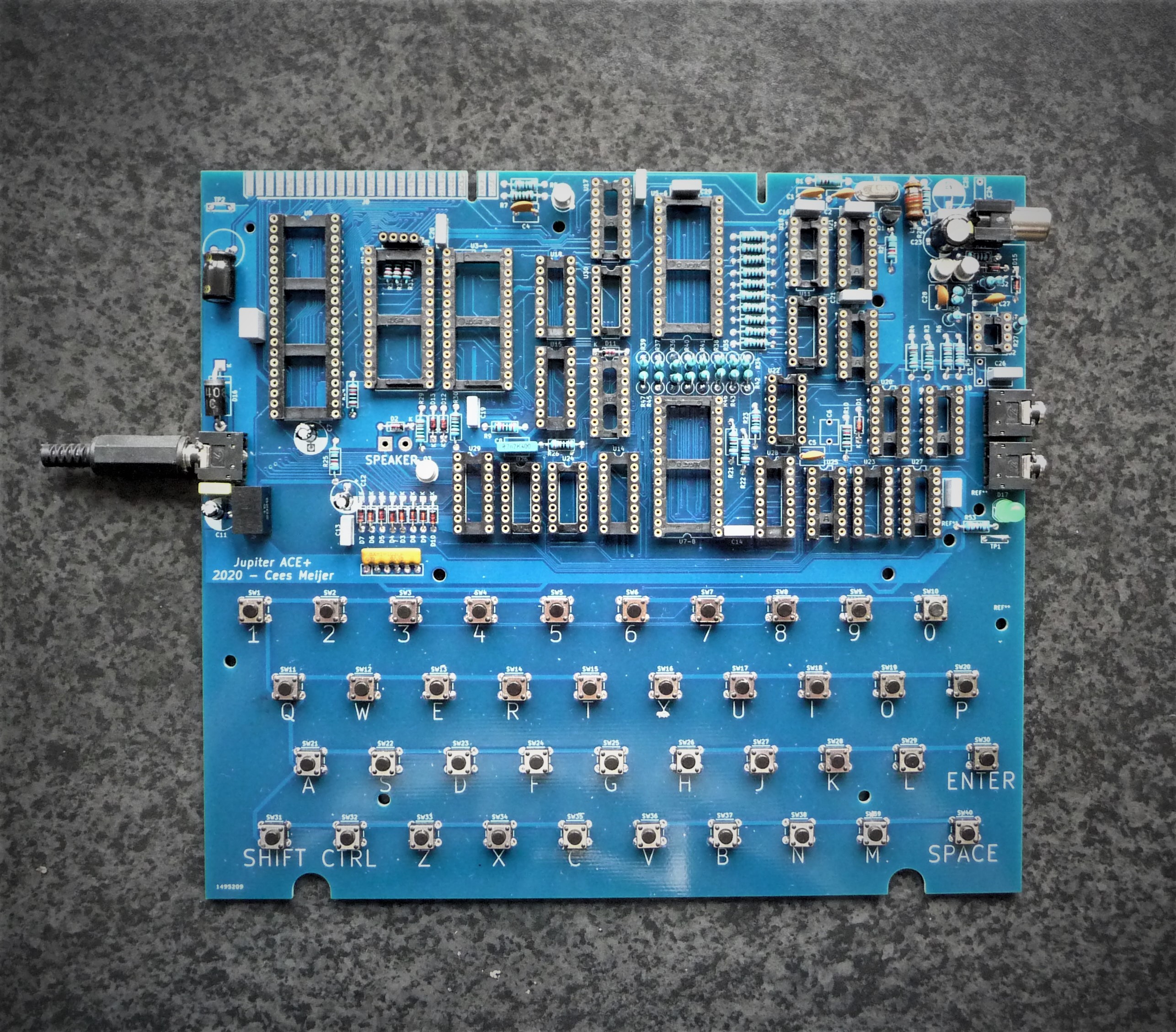
Everything fits like a charm, and it really starts to look like a Jupiter ACE. So it's time to start testing, and carefully insert all chips.
Step 1: Check what is + and - on the power connector. It turns out the Tip is ground, and the sleeve is +. Found myself a leftover power supply (12VDC/1.4A) and mounted the 3.5 mm jack plug. Once connected the LED goes green ! This is always a good start. After that I measured the supply voltage on all main chips like the Z80 and some of the 74 series. All seems well.
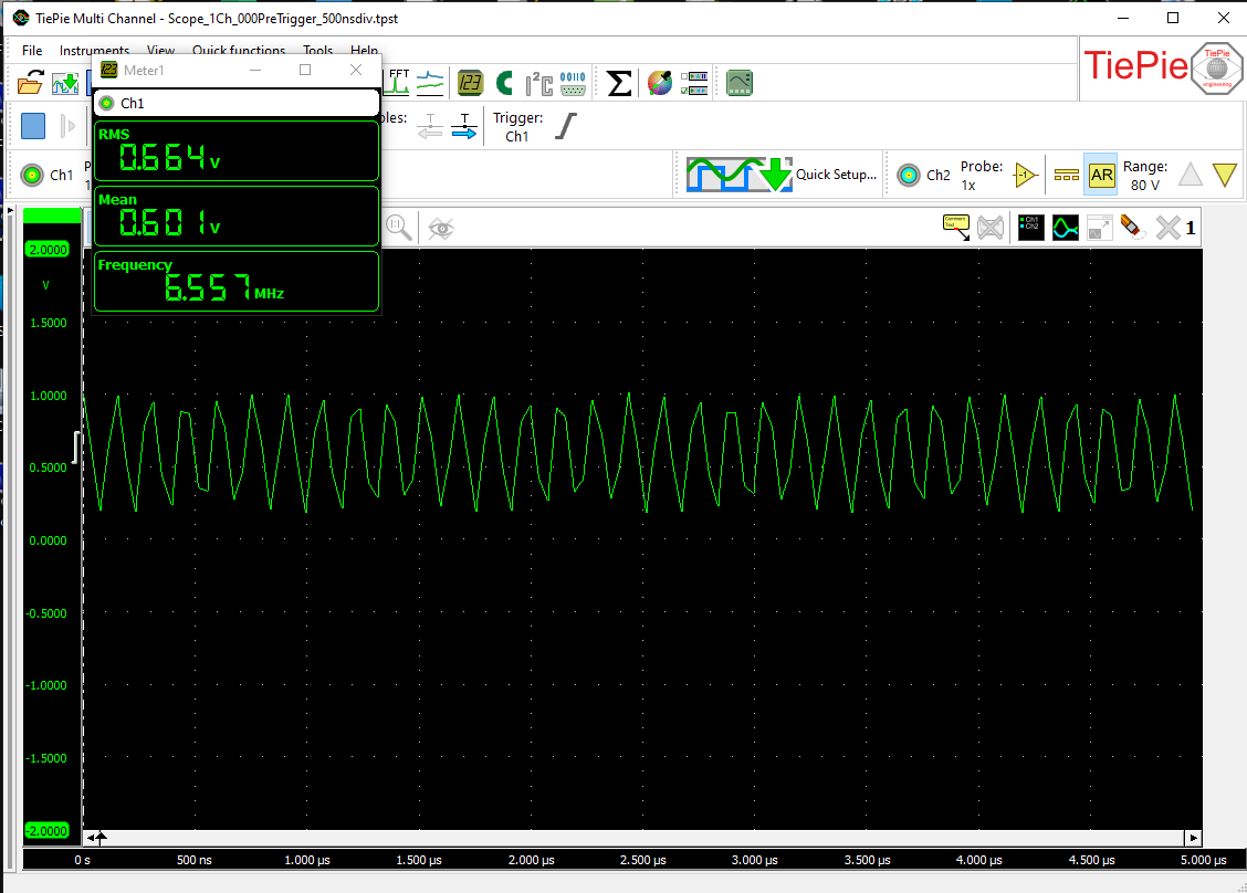
So I first mount U23 74HC86, which is part of the oscillator, so now we should the 6.5 MHz on pin 8.
Which does not happen. There is a clear oscillator signal (with the right frequency) on pin 9, but its simply not big enough:
The signal gets bigger if I replace R2 with a 470K, just enough to get the signal on pin 8 going: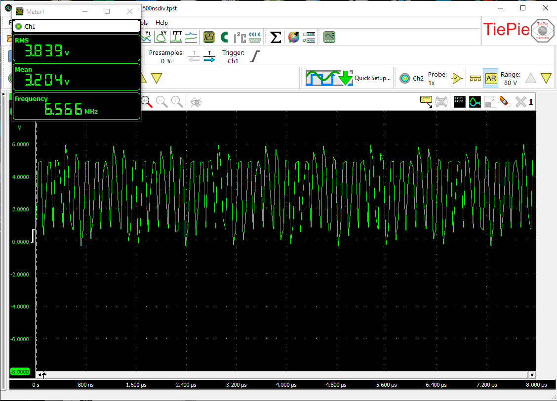 Still looks a bit wacky, but I think that's also a limitation of my oscilloscope which has a maximum sampling rate of 25 MHz so there are only 4 samples per cycle.
Inserting U9: This is the clock signal divider, so there should be a clock on pin3 of U9:
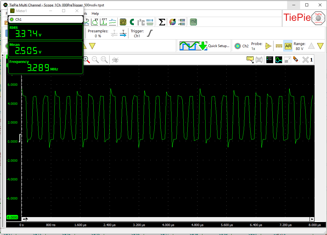 Well, at least it starts looking like a square wave now. So lets insert the next two counters, U10 and U11. Which seems to work as well, so lets mount all other chips. All good, until I came to inserting the RAM chips:
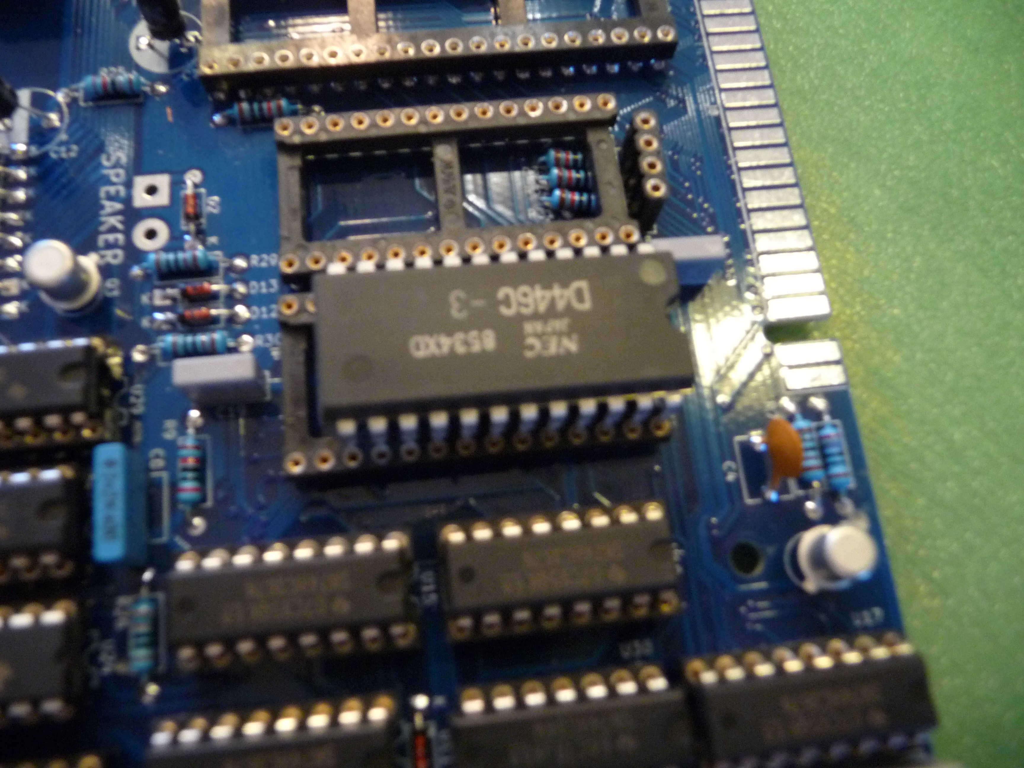
OH NO !! The footprint is wrong. It took me about half a second to realize what was wrong: I selected the DIP28 footprint for this DIP24 chip. Not something KiCad will warn you for, after all the DIP28 has plenty of pins for a DIP24. After about 10 minute of quiet contemplation (...) I decided that I would have to make some kind of adapter with 28 pins on one side and a 24 pin socket on the other so I could re-route all pins from 12 and up.
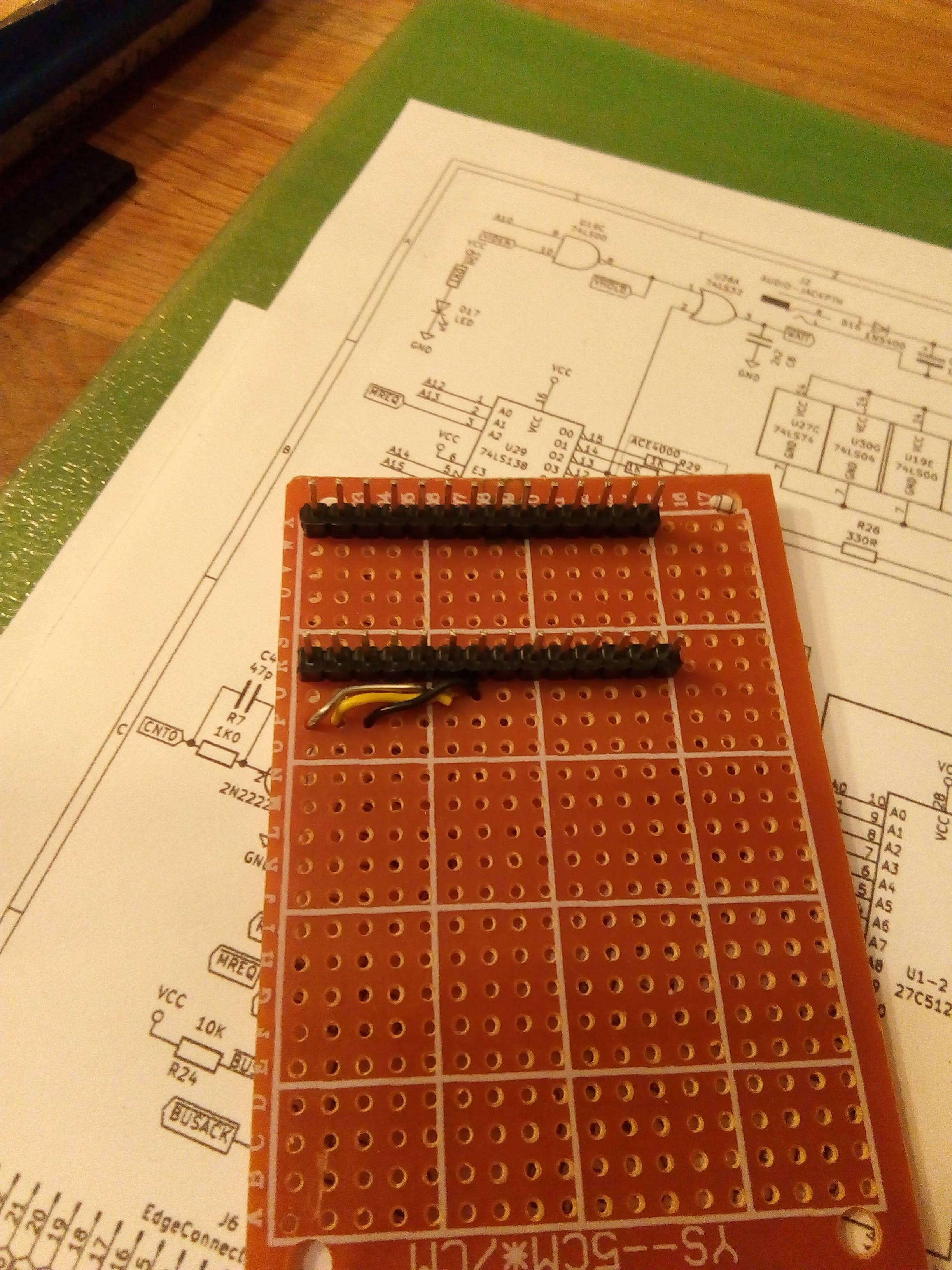
Good plan, but after struggling with the first four wires, and realizing I would have to do 3 adapters in total I gave up. Opened KiCad again and designed an adapter PCB in about 30 minutes. Checked with the PCB manufacturer and found that it would cost €19,- to have 15 pcs manufactured.
So we'll have to wait another week until these boards arrive and the testing can continue.
Discussions
Become a Hackaday.io Member
Create an account to leave a comment. Already have an account? Log In.
Something weird must have happened with those DIP-28 pads; the JEDEC SRAM pinout for DIP-28 is very close to compatible with the DIP-24 pinout. Pins 1-12 are shifted to pins 3-14, and 13-23 to 15-25, so to use a DIP-24 RAM in a standard DIP-28 socket you need plug it into the bottom part of the socket and lift pin 24 and connect it to VCC.
But from looking at your adapter, it seems that you shifted the A7..A0,D0..D2,GND pins upward from their standard locations on a DIP-28 socket?
Are you sure? yes | no
It'll be clear what happened if you look at the pin numbers of the 24 and 28 DIP Kicad symbols and footprints. If installing a 24 pin ROM in a 28 pin socket (which was what the board was designed for), the pins that need to be used are 3-14 on the left and 15-26 on the right, but the 24 pin Kicad symbol will specify pins 1-24.
Are you sure? yes | no
Yeah, I can see that's what happened: A7, which is correctly connected to pin 1 on a DIP-24 footprint, should be connected to pin 3 on a DIP-28 footprint for the same part, but KiCAD still connected A7 to pin 1 on the DIP-28 footprint. What's not clear to me is why KiCAD offers the option to use a DIP-28 footprint for that part with the wrong connections.
JEDEC has standardised both DIP-24 and DIP-28 pinouts for 2K×8 static RAM; when you put the DIP-24 pinout into a DIP-28 socket the only two pins that are different are Vcc and /WE. So if you use a DIP-28 pad for a 2K×8 RAM, you should need to change only those two pins to insert a DIP-24 part. (You can design boards that will work with both pinouts by using DIP-28 sockets and having a couple of jumpers that change DIP-28 pins 23 and 26 between A11 and A13 for DIP-28 parts and /WE and Vcc for DIP-24 parts.)
But I don't know much about KiCAD, so perhaps the issue is really that the part itself doesn't have particular footprints associated with it, simply pin numbers, and KiCAD lets you attach a generic DIP-28 footprint to the part and just wires up the logic to the same pin numbers, without any understanding that A7 is pin 1 on DIP-24 but pin 3 on DIP-28 for that particular part.
Are you sure? yes | no
Yes, I know about the upward compatibility of the 24 and 28 pin EPROMs. The short of it is if you mistakenly use a larger footprint for a symbol, KiCad will not catch your mistake. In KiCad, symbol and footprint are separate concepts. That's logical if you think of a part that is available in more than one package, e.g. DIP16 and SOP16. For example if you use the footprint for a 9 pin resistor network where the schematic only specifies a 5 pin RN, then the additional 4 pads will not be connected. I sometimes take advantage of this "loophole" to allow me to use a longer part in that position if necessary.
For this design the original error was not changing the schematic to use a 28 pin symbol to match the intended footprint, or at least a custom 24 pin symbol with the appropriate pin mappings.
Edit: I see the error was around the SRAM part, I had EPROMs on the brain, but the same idea applies.
Are you sure? yes | no
Ok, so if I'm reading you right, the footprint is baked into the schematic symbol (i.e., there are separate schematic symbols for DIP-24 and DIP-28 2K×8 static RAM, but you still then must manually choose the DIP-24 footprint when using DIP-24 schematic symbol, and if choose a different one it will blindly connect the pins by number anyway? It would seem a bit annoying that KiCAD wouldn't warn you if you choose a footprint that's not the one (or one of the ones) that the schematic symbol must be used with in order for it to work correctly.
Are you sure? yes | no
I can explain. It's not KiCad's fault. I have 'created' the HT6116 RAM myself, and I started from the 27C512. And (unlike most components) apparently this one already had the DIP28 shape assigned to it so I simply forgot to change that.
Are you sure? yes | no
>the footprint is baked into the schematic symbol
Not quite, there is a field for the default footprint in the symbol which can be overriden. As Cees has explained, it got the wrong value from copy and paste of the 27C512 symbol. When completing the symbol fields to move on to work on pcbnew, if I find that the default footprint matches what I am using, I accept that, but I always check that the footprint is the one I wanted.
The other reason for the separation of symbol and footprint, is that there are far fewer footprints than symbols. DIP16 will cover a lot of chips, and TO-92 will cover a lot of 3 pin parts.
Another reason is symbols are at times generic. The schematic may have "4 pin connector" but the actual part could be a 4-pin header, or a Molex connector, or ...
Of course if a component exists in variants with different pin numbering, e.g. DIP40 and PLCC44, then these would be distinct symbols.
Are you sure? yes | no
Yes, I think I see now what's going on here. In my mental model, a schematic symbol for a device has no pin numbers, just lines like A7, and a pin number is part of a schematic symbol to footprint mapping, so that A7 is pin 1 on the DIP-24 footprint mapping but pin 3 on the DIP-28 footprint mapping. But it seems that in KiCAD the pin number is part of the schematic symbol (i.e., you assign A7 to pin 1 on the symbol, rather than in the footprint mapping), so you'd need to have separate schematic symbols for DIP-24 and DIP-28 2K×8 static RAM devices. That's clearly not really the right thing here, but perhaps works better overall.
At any rate, this is why blog posts such as this one are so useful; Cees's pain has probably saved me pain down the road!
Are you sure? yes | no
There is another reason for having pin numbers (or rather pin IDs) on symbols. KiCad allows you to specify the pin property (input, output, tri-state, bidirectional, power input, power output, passive, NC, etc) for the electrical rule checker, which helps catch mistakes in schematic design.
Are you sure? yes | no
To be extra-clear here, I am indeed suggesting that there be PIN IDs, such as "A7," which can have properties assigned for the electrical rule checker as you point out. I'm just saying that there's no need to associate these with pin _numbers_ in the schematic symbol; that could be done in a separate schematic-symbol to footprint mapping.
Are you sure? yes | no
Yes, I suppose you could associate properties with pin labels and get rid of the number/ID field. Then the trade-off would be work to associate symbols with numbered footprints so that library would need to have the various mappings. The other field you would have to assign at that point is the component name. Usually when drawing a schematic you start from a known component name like HT6116, rather than 2k*8 SRAM. (The library allows aliases, and in v6, inheritance, so there is already grouping.) Manufacturer datasheets still use numbers, there are not that many components that have more than one function-pin mapping so separate symbols isn't a large overhead, so it's not unreasonable to use numbers from the start. A place you will see a lot of apparent duplication is in transistor symbols like Q_NPN_EBC and Q_NPN_ECB, and so forth.
Pin numbers are still useful even at the schematic stage. Placement is a significant part of the work prior to routing. If I spot from the numbers that choosing a different port assignment on an MCU will give a more compact routing, I can do that. I can also do things like change the unit for parts that have multiple units, e.g. logic gates.
Anyway this is how KiCad entities are organised. It generally works. Other CAD programs may organise things differently.
Are you sure? yes | no
There are other practical issues with using pin labels as identifiers. In modern MCUs, often pins have multiple functions which can be assigned dynamically, Take the example of the STM8S103F3 in the SDIP32 package. Pin 23 is labelled PC1 (HS)/TIM1_CH1/UART1_CK. Which one of the functions should be the label? All of them? That's quite a long label. At least pin numbers/IDs are short and uncontroversial. Given that each package exposes a different subset of the chip connections, it's no big deal to have separate symbols for say the TSSOP20 and the SDIP32 package. The designer is not likely to change the package mid-design. It was simpler in the days when you could say, that's pin A7.
Are you sure? yes | no
Well, if you take the idea through its logical implementation, I think a lot of the things you suggest are problems aren't really, or are no worse than the existing ones.
Yes, of course the library would have sets of mappings to footprints, rather than the single mappings to pin numbers and the default footprint a symbol has. That's exactly my proposal. When you choose a device by name, it would bring in a symbol and footprint, as it does now; the only difference is that it wouldn't have a different symbol that mostly duplicates another symbol when you choose one of several available footprints. (DRY in action here.) There's no reason it couldn't show the pin numbers at the schematic stage, and the nice thing would be that the pin numbers would correctly change on the schematic if you changed the footprint. Changing individual units from things like a quad NAND would work just as it does now, except the names of the pins would be more clear (2A, 2B, 2Y instead of 4,5,6 or 6,7,5 or 6,8,9 depending on which SN74xx00 package you chose). For multifunction pins, if you want a short label just choose one function; "PC1 (HS)" is still a lot more clear and less error-prone than "17" even if it's being used in an alternate role.
Are you sure? yes | no
Well I think your scheme doesn't have an advantage over the current one to change over to. All you're getting for it is the ability to use generic symbols that might have different mappings. It only benefits a tiny portion of the chips on the market, like logic chips and memory, and some that exist in two pinouts, like the 74LS373 and 74LS573. Designers usually start from a known model rather than saying I want 4 NANDs, but I won't commit to a package until later. A couple of times I switched from the 373 to 573 or the reverse and it was no big deal just to replace the symbol and redo the routing. Then you are also asking symbol maintainers to maintain two pieces of information, the symbol, and the mapping, in different places.
As for choosing just one function of a MCU pin as the ID, sorry I can't take you seriously on that.
BTW since you don't seem to be a user, you are aware that eeschema also shows the label of the pin in addition to the number? Plus any other visual hints from the shape of the symbol, e.g. NOR gate shape, circles on inverted outputs. So it's not as if you only see the number on the schematic and not the function. All that you are proposing is to index on the label and have late binding to the number (or ID, as some "numbers" are actually strings like G24, for grid pinouts).
But I'm not a KiCad developer or even an expert, just a user, so instead of clogging up Cees' page, I encourage you to go to the KiCad forum and post there, if you feel strongly about this.
Are you sure? yes | no
"...I can't take you seriously on that."
Sorry, I must have misunderstood you, then. I understand why you feel that "PC1 (HS)/TIM1_CH1/UART1_CK" is too long, but you seemed to be proposing that "23" is a better label than "PC1 (HS)" or whatever when trying to keep labels shorter. I think someone's a lot more likely to make an error with "23" than with almost anything else, even if the label they're using is an alternate function, especially when they have to remember that "23" is actually "37" on a different part.
So I honestly don't understand what you're saying to use, there, if you don't want to use function labels. What else is there but pin numbers, then?
As for the rest, yeah, I know that one can show labels as well as pin numbers, and even assign bus/signal labels and so on. I just don't see why it's better to have the "canonical" label for a function be a random number that changes from part to part rather thant the name of the function.
Are you sure? yes | no
I encourage you to spend some time with KiCad instead using your mental model of KiCad. You seem to be under the misapprehension that all you see in eeschema is the pin number and that you're liable to make a mistake relating that to the function. In fact both the number and the label are visible. Have a look at one of my schematics here: https://github.com/kenyapcomau/89c52-board/blob/main/89c52board.pdf and see for yourself that both the pin number and function are shown. This particular MCU comes in DIP40 and LQFP/PLCC44 so probably different symbols are required. However the same symbol can be used for both the 89C51 and 89C52 variants which only differ in flash memory size. In fact if you have a keen eye you will see that I derived that symbol from the 8051 one and was too lazy to change the model name.
Your scheme simply boils down to late binding of the number but this only allows grouping for a minuscule number of components for more steps by the user. In the current scheme the user chooses the component model which has a certain pinout. This is easy to relate to. You would ask the user to choose say 2k RAM then choose the model in a later step. More steps for a insignificant saving in storage and more data to keep consistent
Please also distinguish between id and label. Label is the meaningful acronym for the function(s). There is another kind of label which is net label. That's a different animal, as is bus label. Id is the pin number. In database parlance it's the primary key.
Currently if I want a 2k RAM I choose the model up front. Why delay that decision? Usually the designer already knows which parts they are working with. Naturally the system copes with aliases like 6116/2016 etc.
Are you sure? yes | no