 Bud Bennett
[Edit 2019-06-29: entire log was scrapped and replaced. I was totally wrong about how to go about analyzing the various noise contributions to the output of the circuit. I may still be wrong, but I think the following analysis is on the correct path.]
The purpose of this exercise is to analyze the circuit topology to determine the contribution of each source of noise and then select component values that minimize the overall noise at the circuit's output. The goal is to keep the peak-peak noise level below the amount necessary to guarantee 22-bits of dynamic range from the ADC.
The positive and negative signal paths use identical circuitry -- it is only necessary to calculate the noise in one path and then mulriply by √2 to get the total noise at the differential outputs. The demodulator appears to be essentially noiseless -- consisting of a small switch resistance -- so I will ignore it.
I determined that the best approach was to insert a pseudo noise source into the simulated circuit and see what how the noise source affected the output voltage. Then it is a matter of just adding up all of the noise contributions to get the total.
Noise contribution of U7:
I inserted a voltage source, EN7, to see what the voltage noise of U7 contributed to the output voltage. (This is not the circuit used for simulation. It is just an equivalent schematic.)
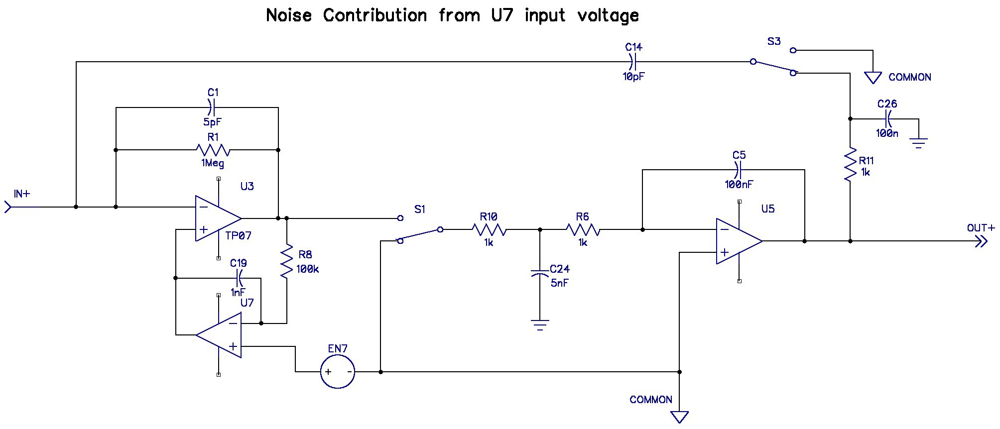
I made EN7 a sinewave source with a magnitude of 10mV peak. EN7 emulates the equivalent input voltage of the opamp U7. The simulation produced the following ouput.
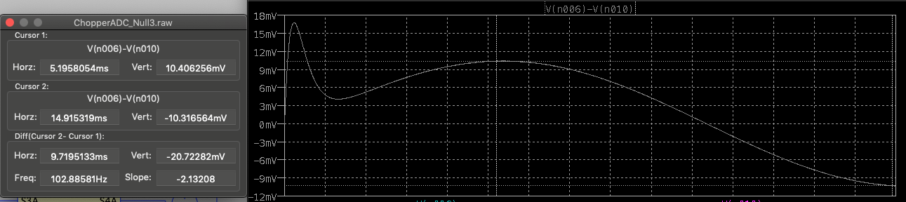
The simulation indicates that the gain from EN7 to the output is 2.072 V/V. The noise contribution is present at DC and also at the modulation frequencies and its harmonics. Therefore U7 should probably be a zero-drift chopper amplifier that has no 1/f noise component at DC.
I found through simulation that the value of C1 should be as small as possible, and R1 should be large, to minimize the noise contribution of U7. But R1 is also a noise source that should be minimized as well.
Noise contribution of U3:
I inserted a voltage source at the positive input of U3 to simulate its contribution.
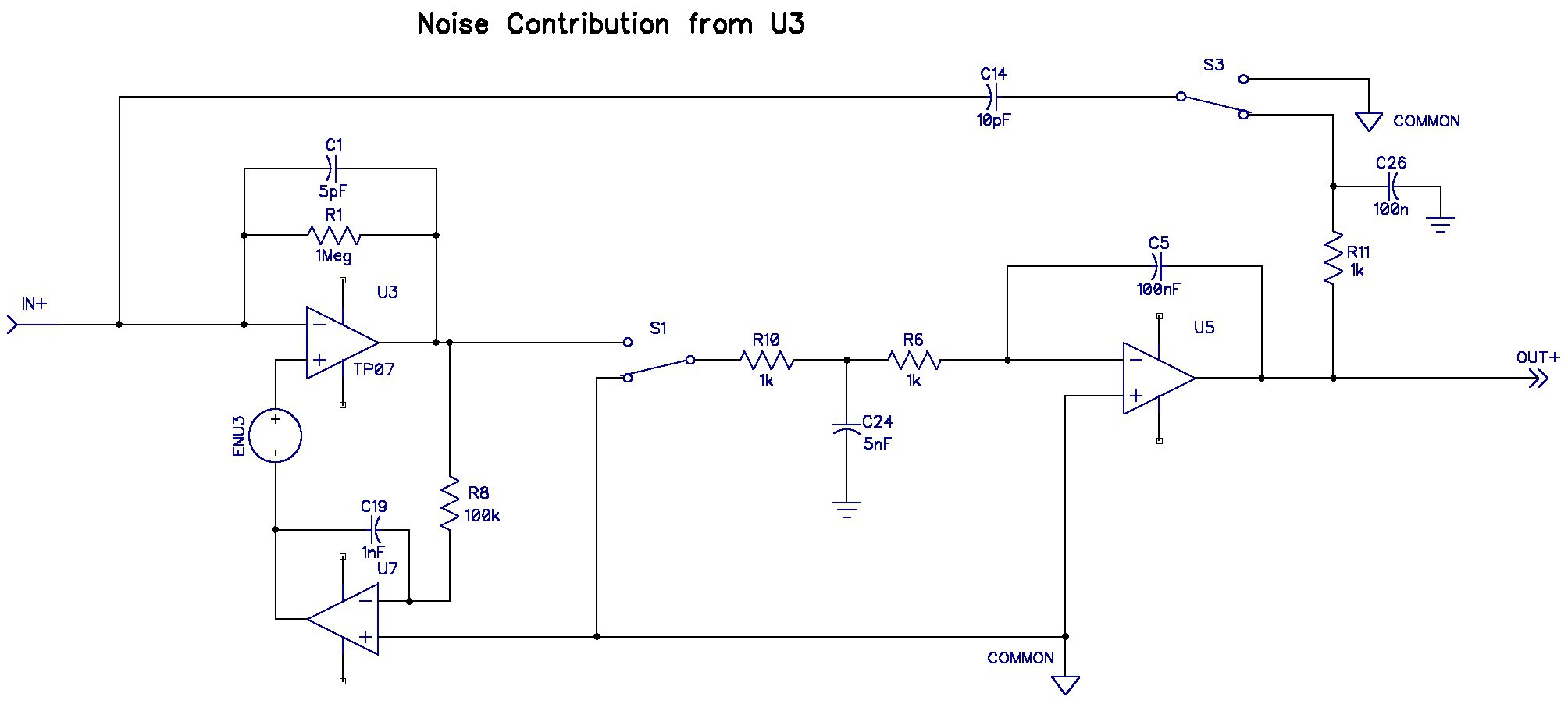
The simulation indicated that there was no significant low frequency noise contribution from U3 because U7 removed it. Unfortunately, the input voltage noise of U3 is not reduced by U7 at the 100kHz modulation frequency. The gain to the output from EnU3 at 100kHz is 2.84 V/V. I found this out by increasing the frequency of EnU3 to 100.050kHz and measuring the amplitude of the resultant waveform at the output. U7 should have low input voltage noise at frequencies above 90kHz.
Noise Contribution of R8:
The noise voltage source is now in series with R8 to simulate its contribution to the output.
The noise from R8 only contributes at DC with a gain of 1. The takeaway: make R8 as small as possible.
Noise Contribution of R1:
A voltage source is inserted in series with R1 to estimate its contribution to the output.
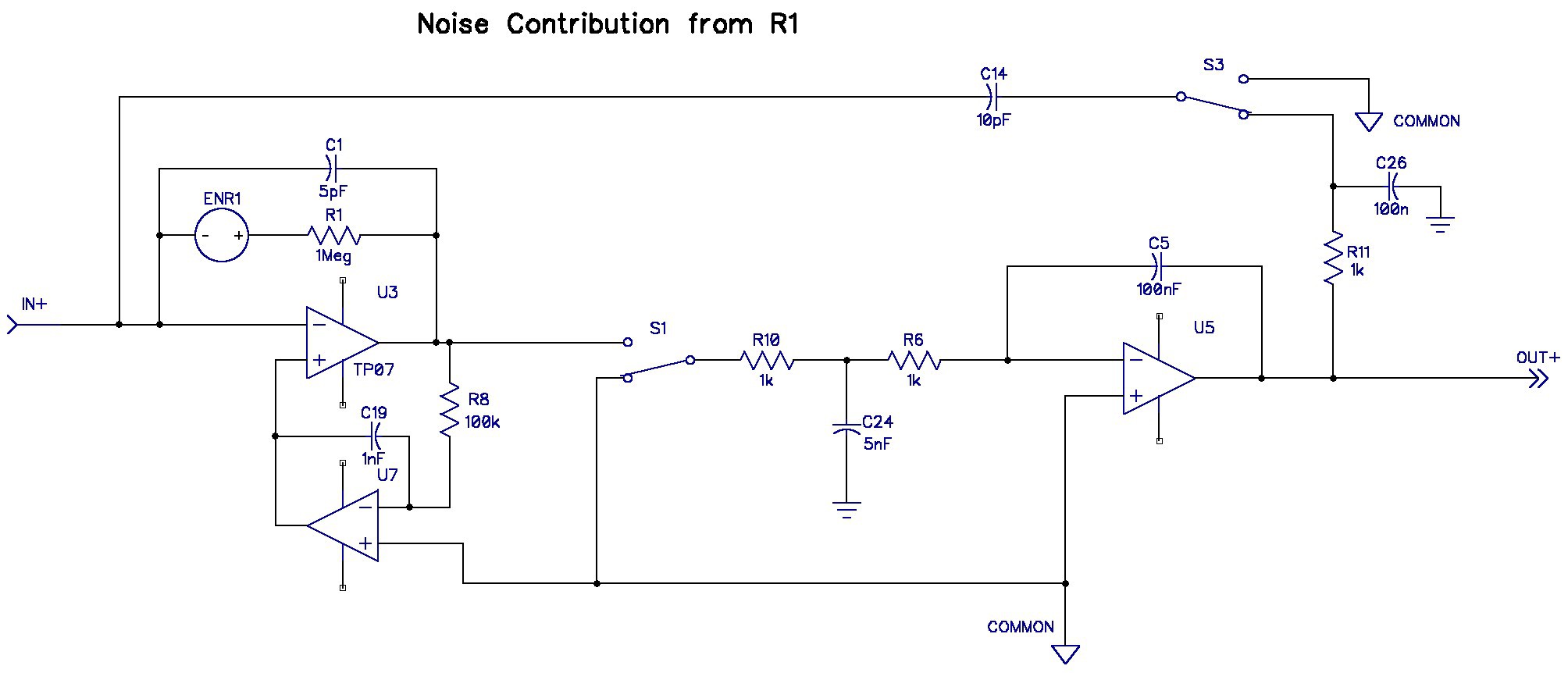
The gain from R1 to the output is 0.2 V/V at 100kHz and harmonics. U7 removes the noise at DC. The tradeoff here is to make R1 as large as possible, to reduce noise from U7, but not so large that its thermal noise dominates.
Noise Contribution of U5:
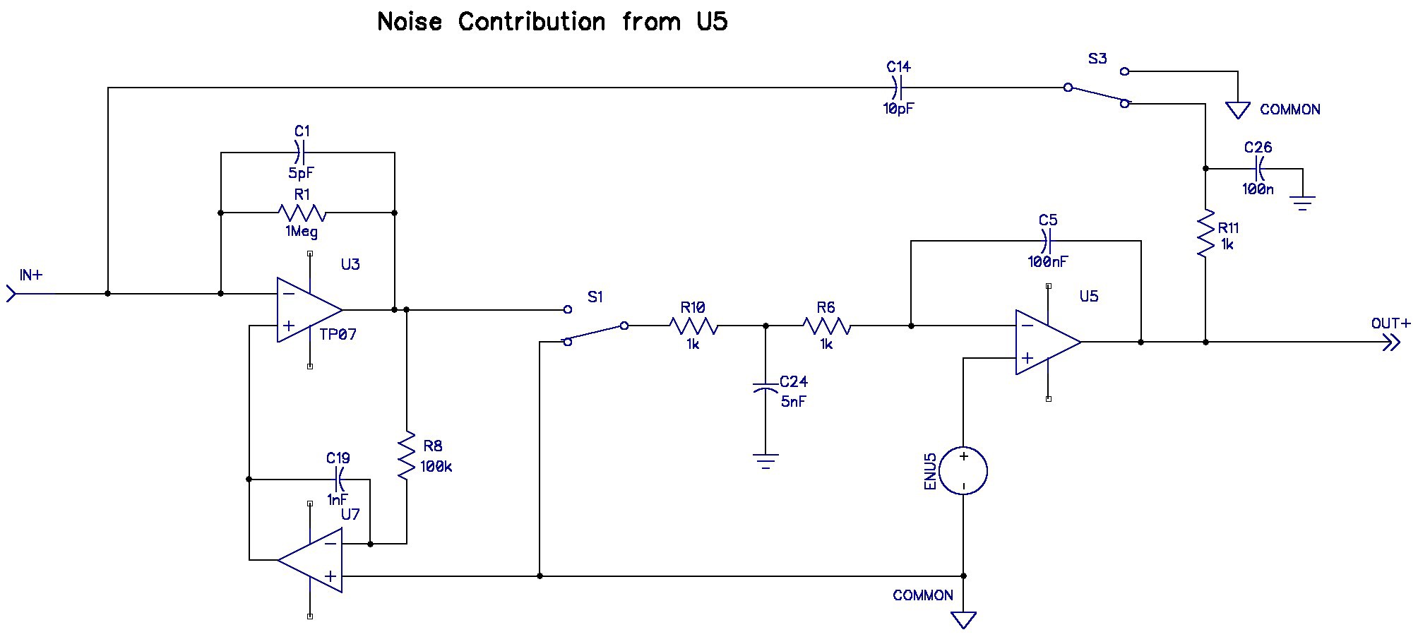
The simulation indicates that the gain from ENU5 to the output is 2.2 V/V. This noise is only injected at DC.
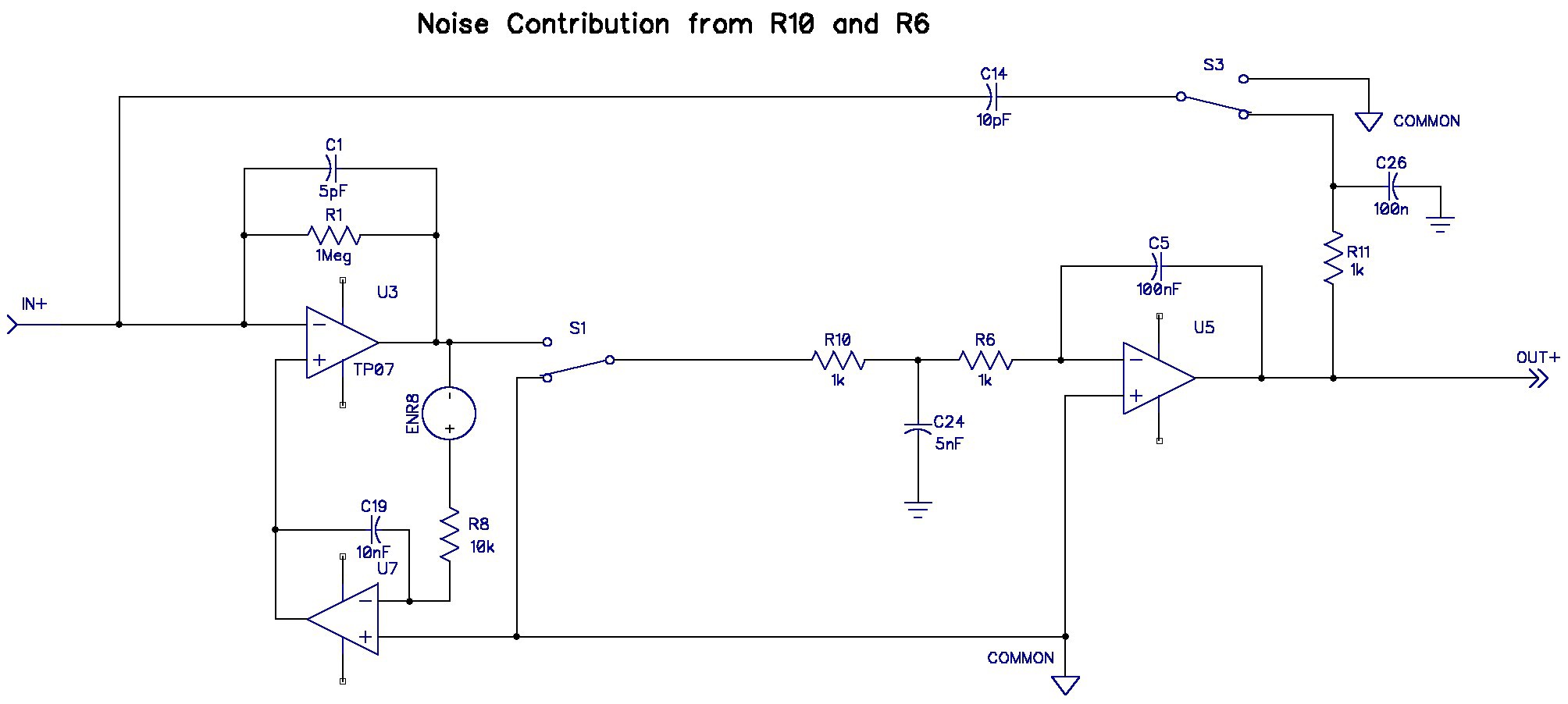
Noise Contribution of R10 and R6:
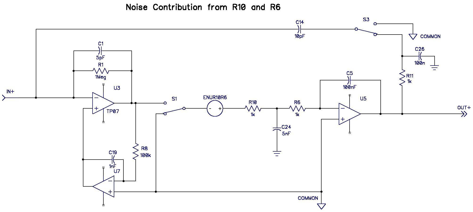
Simulation predicts the gain from these two resistors ( at DC) to the output is 2.16 V/V.
Putting it all together:
The individual noise components are assumed to be independent, therefore they can be added by superposition.
[Edit 2019-07-11: Noise at 100kHz and the 3x harmonic are uncorrelated. Therefore the noise components at different frequencies must be squared and added. ]
Noise at the output of the positive signal channel is the sum of the square noise components:
VnOut^2 = (EnU7*2.2)^2*(1^2 + 1^2 + 1/3^2) + (EnU3 * 2.84)^2 * (1 + 1/3^2) + EnR8^2*(1 + 1/3^2) + (EnR1 * 0.2)^2 * (1 +1/3^2) + (EnU5 * 2.2)^2 + (EnR10R6 * 2.16)^2
Note that terms multiplied by 2.33 are present at DC and the modulation frequency plus harmonics. If the term is multiplied by 1.33 then the DC content is removed by U7, but is present at the modulation frequencies.
From the datasheets of the OPA376 and MCPV81:
EnU3 = 7.5 nV/√Hz, EnU7 and EnU5 = 13 nV/√Hz.
Calculated thermal noise of R1 and R8:
EnR1 = 127.2 nV/√Hz
EnR8 = 12.72 nV/√Hz
EnR10R6 = 5.7nV/√Hz
Therefore, the total rms noise density of the total differential output is
VrmsOut = √2*sqrt( (13nV * 2.2)^2 * (2.11) + (7.5nV*2.84)^2 * (1.11) + 12.72nV^2*1.11 + (127.2nV*0.2)^2 * 1.11 + (13nV*2.2)^2 + (5.7nV*2.16)^2 )
= 90.5nV/√Hz.
The MAX11200 ADC has an input referred noise of 575nVrms when sampliing at 10Hz. We can infer a noise density by dividing the input noise by √5Hz, the Nyquist frequency, to get 257nV/√Hz. Adding the noise of the chopper amplifier to the ADC yields:
VrmsTotal = sqrt(90nv^2 + 257nV^2) = 272nV/√Hz.
To obtain peak-peak noise multiply by a factor of six and the sqrt of the signal bandwidth:
Vp-p = 6 * 285nV = 1.63µVp-p for a 1Hz bandwidth.
Expected noise-free dynamic range is then:
NFDNR = 2 * 0.8 * VCC/1.63µV = 3.53 x 10^6 = 131dB, or 21.8 bits.
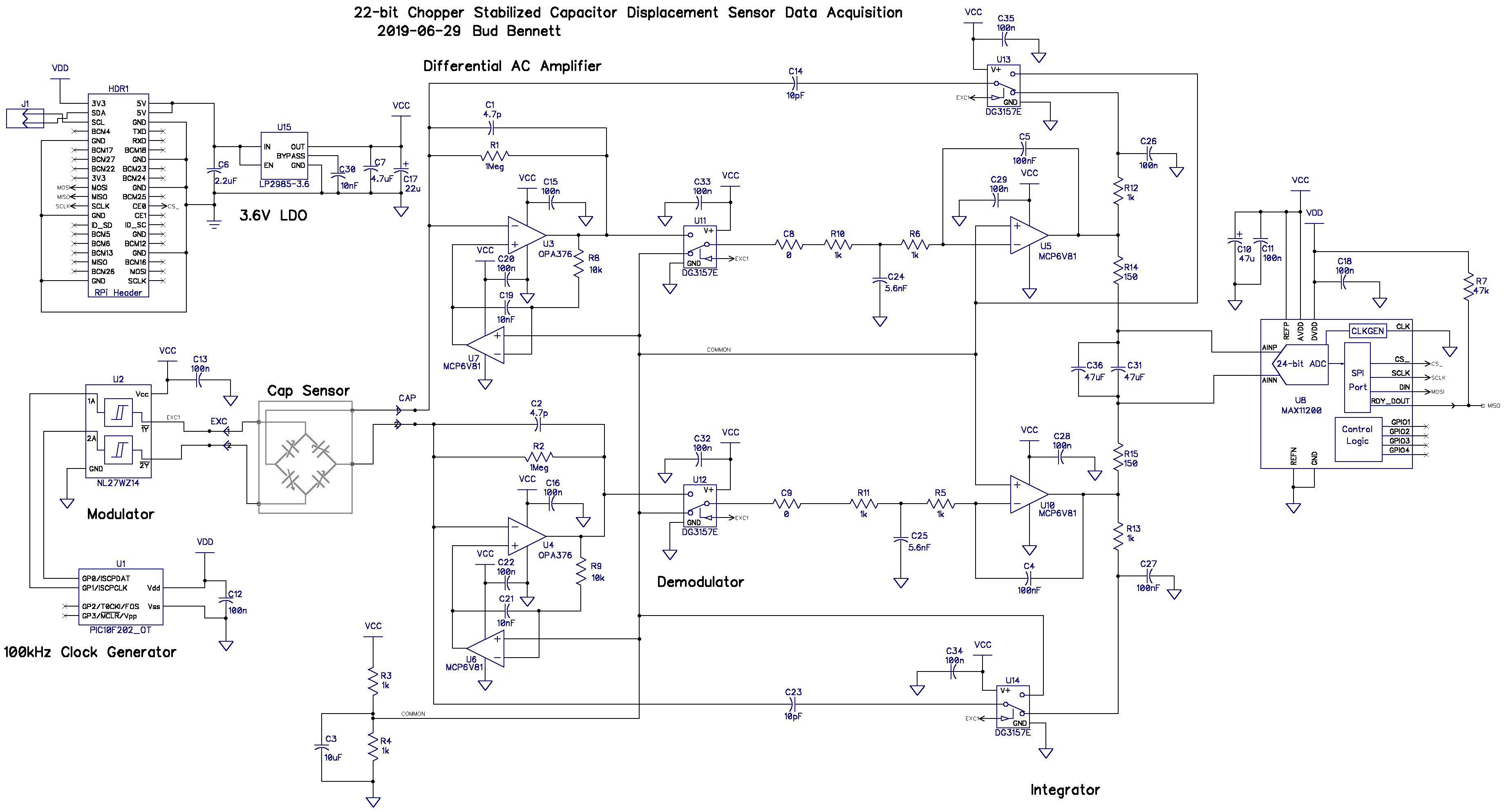
The noise optimized schematic at this point in time looks like this:
Discussions
Become a Hackaday.io Member
Create an account to leave a comment. Already have an account? Log In.