 Bud Bennett
This idea originated from L.K. Baxter's "Capacitive Sensors" paper, which I have included in the files section of this project. Baxter covers signal conditioning in Chapter 5, but only using block diagrams. This is the diagram of a simple synchronous demodulator from the paper ( I implemented this as a first pass.)
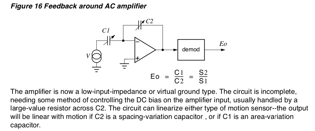
But it was this block diagram, which I call a nulling feedback demodulator, and his comments that I did not immediately understand in any meaningful way:
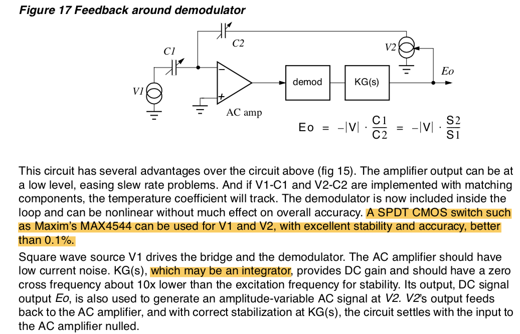
He is using current source symbols for AC voltage sources. It was unclear to me how V2 was implemented, but the highlighted comment about the SPDT CMOS switch is the clue. V2 is a voltage variable AC source controlled by the output of the integrated demodulator signal. I eventually understood enough to translate the above diagram into this simple differential circuit concept to use with my cap sensor:
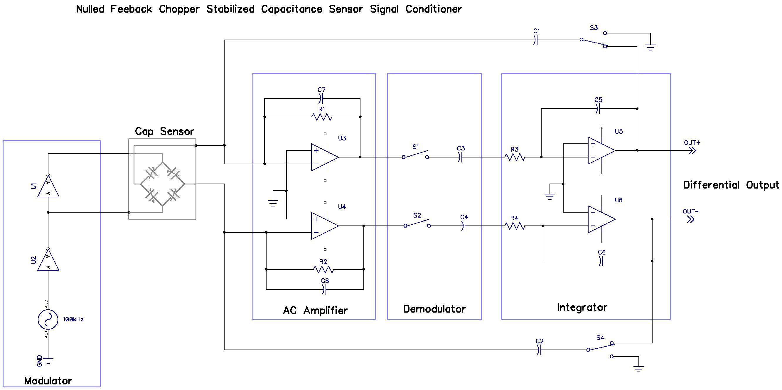
All of the switches are in phase with the modulator. This circuit includes capacitors in the demodulator to eliminate the DC terms present in the AC amplifier that should get removed by the chopper operation.
The overall gain of the circuit only depends upon the cap sensor, the feedback capacitors C1 & C2, and the excitation voltage, which is the supply voltage:
Vout = (∆C/C1 - -∆C/C2) VCC = 2∆C/C1 VCC = ±VCC/2 , for ∆C =±4pF, C1 = C2 = 16pF.
In order to more fully understand the operation of this circuit I simulated it using LTSpice. The LTSpice schematic is too messy to present here, but the simulated signals lend some understanding of what the circuit is doing and the sensitivities of the component values on the circuit performance.
Without the nulling feedback the AC amplifier outputs are required to slew and settle to large differential outputs, as shown here for a full scale cap sensor ∆C.
The amplifier (a simulated ADA4500, with a 16pF and 10Meg for feedback elements) must get to the final output voltage and then settle quickly before the end of the sampling period, in this case 2.5µs. The sloped square waves are caused by the resistor used for DC bias that is discharging the capacitor during the interval -- this causes a gain error.
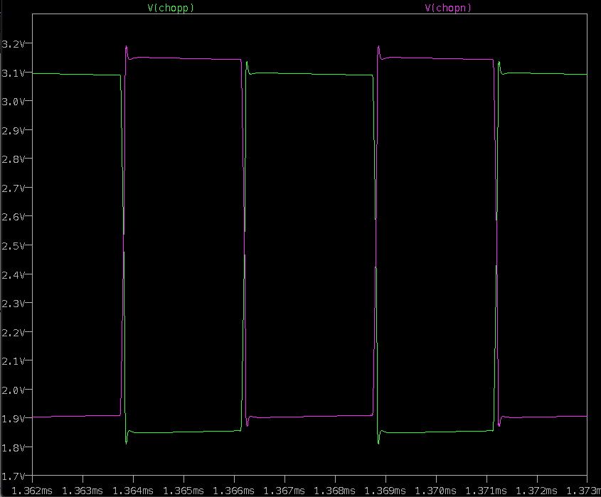
Here's the what the amplifier outputs look like when producing the same full scale ∆C when nulled in a steady state with a 100kHz excitation frequency:
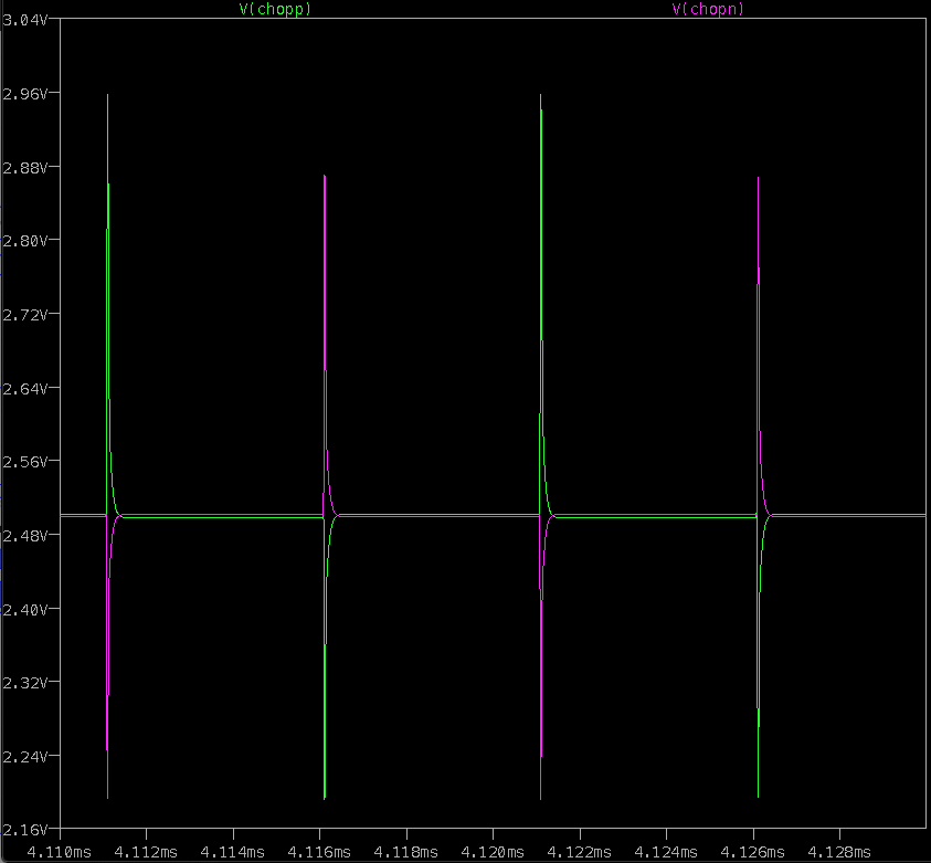
The simulated amplifier is the same ADA4500, with 10pF and 10MegΩ feedback elements. There is an initial spike when the charge on the capacitors is applied to the amplifier inputs, but since the charges are nearly equal the amplifier settles to a low output voltage and there is very little error produced by the 10MegΩ feedback resistor -- eliminating the gain error due to discharge. Baxter is correct in claiming that a lower bandwidth amplifier can be used, with lower slew and settle requirements. In addition, the resistor feedback element used for DC bias can be made lower, which reduces the sensitivity to leakage currents at the inputs. But it doesn't eliminate it.
I got a shock when I simulated a 10nA leakage current injected into the input of one of the AC amplifiers. The leakage current produced a 100mV error in the output voltage. After a long struggle to understand and fix the problem I implemented the following circuit.
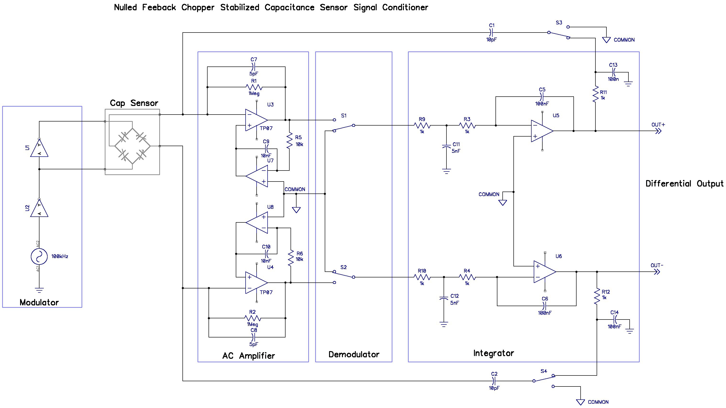
The leakage current created a DC voltage across the AC amplifier. Because the Demodulator switch samples only one edge of the AC amp output a DC component would appear to get passed through to the output because the charge at the input was not properly cancelled. The integrator wrapped around the AC amplifier sets the average output voltage of the AC amp to equal the common voltage node. Now the simple switch in the Demodulator has no offset voltage to develop any DC voltage at its output. This scheme works really well: using 100kΩ resistors to set the gain of the AC amplifiers, the output error to a huge 1µA leakage current at either input will only develop 33µV of error at the differential outputs! And because the AC amps don't develop any significant output voltage there is plenty of common mode range.
I also removed the capacitors in the Demodulator. There is no longer a DC component in the signal, except for the residual offset and offset drift of the input integrators. And it was eventually apparent to me that there was no DC path to bias the output integrator if the capacitors remained in the Demodulator.
There are a few additional passive components sprinkled around the circuit. They are necessary for good performance.
- The high frequency RC filter in front of the output integrators are designed to swallow the short pulses from the demodulator so that the integrator doesn't have to deal with them.
- Similarly the RC between the output and the switches that generate the AC feedback voltage is there to prevent any glitching from the capacitor discharging into the input from affecting the integrator output.
There are a number of general notes about the components:
- The AC amps remain relatively high performance TP07 for now. It might be possible to use slower opamps with poorer specs.
- The four opamps that perform integrator functions are nothing special to get good DC performance. I expect that these opamps will be selected based upon their noise performance
- The switches S1 and S2 can be discrete SPST analog switches, unless they need low charge injection. Simulation required.
- The S3 & S4 switches are SPDT and are available in single and dual per package. There are similar issues with charge injection. Many analog switch ICs don’t specify charge injection so the selection process might be difficult if low injection is required.
- The output integrators are low impedance and can replace the input buffers in the MAX11700 ADC. This might be a good noise performance tradeoff.
- C1 and C2 must be C0G or NP0 with tight (1%) tolerance. I might reduce their values to increase the output voltage range to near ±VCC if the ADC can handle it.
The next step is to finish up a few loose ends on this concept and then perform a noise analysis. More stuff in the next log.
Discussions
Become a Hackaday.io Member
Create an account to leave a comment. Already have an account? Log In.