 Sander van de Bor
Most of us start off with the Arduino UNO, but after a while you might try out more advanced boards, or boards from other suppliers, and you must add these board to the board manager. You might end up like me with an endless long list of boards. Adafruit boards, ESP32 and ESP8266, ATtinyCore etc.
I will not go into details how these are created, but when you are interested in the process and want to learn more, there is a good description in the wiki section of the Arduino Github page:
https://github.com/arduino/Arduino/wiki/Arduino-IDE-1.5-3rd-party-Hardware-specification
I have done multiple custom boards before. Added the Micronucleus bootloader to SpenceKonde ATTinyCore; created custom M0+ board and my latest was a custom board with an ATSAME54N20A based on the Metro M4 from Adafruit. So adding a custom variant to MegaAvr should be a piece of cake, at least that was what I thought.
Each board in the board manager has a variant file where mainly all Arduino related naming is linked to a pin, timer, output etc. by mainly using macros. At least, it used to be like that. The MegaAvr variant file still contains a lot of macro’s, but some information is actually stored in the flash memory if the micro-controller. Something new to get used to. The files in the variants folder are named different as well and do contain some additional information. All this information is spread over the following file which you can find in the variants folder for the Arduino Uno WiFi Rev2 and Arduino Nano Every:
- pins_arduino.h
- timers.h
- variant.c
To be flat out honest with everybody, I don’t know where the timers.h is used for (something with time tracking, but isn’t that the Real Time Counter (RTC)?), and the variant.c is currently going over my head and need some more time to understand, so for today I will only focus on pin_arduino.h
When you write to a pin number in Arduino, you are actually setting a bit in a so called PORT. Each PORT is a register, and the length of that register is determined by the type of micro-controller you are using. For example the Arduino UNO is 8 bits, so each PORT controls 8 I/O pins. Since the ATMEGA328P, the micro-controller used on the Arduino UNO, has 23 I/O pins it needs at least 3 registers to control all of these. PORTB controlling 8 I/O pins, PORTC 7, and PORTD 8. You are probably wondering what happened to PORTA. I do not know, but I am sure Atmel at that time had a good reason to start at PORTB, probably because it is sharing the same architecture with other (larger) controllers where PORTA was required for additional I/O pins. While most 32 bits micro-controller have more I/O pins, they require less PORTS since each port can control 32 I/O pins. For example the ATSAMD21G18A, used on the M0, has 38 I/O pins, but only 2 PORTS.
So each PORT is identified by an alphabetic letter and each pin with a number, starting at 0, which will result in pin identifications like PB5, PORTB pin number 5 (keep in mind this is the sixth pin). This concept is important to understand when we start working with the pin_arduino.h file.
We will use the pin_arduino.h located in the C:\Users\username\AppData\Local\Arduino15\packages\arduino\hardware\megaavr\1.8.1\variants
The code start as follows:
#ifndef Pins_Arduino_h
#define Pins_Arduino_h

#include <avr/pgmspace.h>
#include "timers.h"

#define NUM_DIGITAL_PINS            22 // (14 on digital headers + 8 on analog headers)
#define NUM_ANALOG_INPUTS           14
#define NUM_RESERVED_PINS           6  // (TOSC1/2, VREF, RESET, DEBUG USART Rx/Tx)
#define NUM_INTERNALLY_USED_PINS    10 // (2 x Chip select + 2 x UART + 4 x IO + LED_BUILTIN + 1 unused pin)
#define NUM_I2C_PINS                2  // (SDA / SCL)
#define NUM_SPI_PINS                3  // (MISO / MOSI / SCK)
#define NUM_TOTAL_FREE_PINS         (NUM_DIGITAL_PINS)
#define NUM_TOTAL_PINS              (NUM_DIGITAL_PINS + NUM_RESERVED_PINS + NUM_INTERNALLY_USED_PINS + NUM_I2C_PINS + NUM_SPI_PINS)
#define ANALOG_INPUT_OFFSET         14
It uses some macros to name some variables which are used throughout the Arduino Core. The NUM_DIGITAL_PINS and NUM_ANALOG_INPUTS are pretty straight forward; it is the number of pins on the board which are used for digital I/O followed by the number of pins used for analog input. This is not much different from previous boards, but some of the other identifiers are new to me, like the NUM_TOTAL_FREE_PINS and ANALOG_INPUT_OFFSET. It is not important at this moment and I will get back to it after I figure it all out.
Let’s go down to line# 118. Here you can find a graphical ASCII representation of the ATMEGA4809 micro-controller with a label for all the pins.
//                     (SCL)(SDA) (7)  (2)                 (R)  (3~) (6~)
//                 PA4  PA3  PA2  PA1  PA0  GND  VDD  UPDI PF6  PF5  PF4  PF3
//
//                  48   47   46   45   44   43   42   41   40   39   38   37
//              + ____ ____ ____ ____ ____ ____ ____ ____ ____ ____ ____ ____ +
//        PA5   1|                                                             |36  PF2
//        PA6   2|                                                             |35  PF1 (TOSC2)
//        PA7   3|                                                             |34  PF0 (TOSC1)
//   (9~) PB0   4|                                                             |33  PE3 (8)
//  (10~) PB1   5|                                                             |32  PE2 (13)
//   (5~) PB2   6|                                                             |31  PE1 (12)
//        PB3   7|                          48pin QFN                          |30  PE0 (11~)
//   (Tx) PB4   8|                                                             |29  GND
//   (Rx) PB5   9|                                                             |28  AVDD
//        PC0  10|                                                             |27  PD7 (VREF)
//        PC1  11|                                                             |26  PD6
//        PC2  12|                                                             |25  PD5 (A5)
//               + ____ ____ ____ ____ ____ ____ ____ ____ ____ ____ ____ ____ +
//                  13   14   15   16   17   18   19   20   21   22   23   24
//
//                  PC3  VDD  GND  PC4  PC5  PC6  PC7  PD0  PD1  PD2  PD3  PD4
//                                 (1)  (0)  (4)       (A0) (A1) (A2) (A3) (A4)
The leg number of the pin is closest to the board, for example 4, followed by the pin identification PB0 (PORT B, first pin), and some have a number or description in parentheses, in this case 9~. 9 is the actual pin number on the board, and the number used in Arduino. In Arduino, digitalWrite(9, HIGH) will turn on PB0. The tilde (~) next to the 9 is there to identify that this can be used as an PWM output. PWM requires timers to setup, so I will get back to that later as well.
The ATMEGA4809 has 41 I/O pins, so needs at least 6 PORTS, and looking at the drawing we see that PORTA up to PORTF are used for that.
Underneath the graphical representation of the board there are some arrays created to be stored in Flash memory. The first array, digital_pin_to_port, only list which PORT each pin belongs to. The order of the array is important, because it is in order of the Arduino pin assignment. Like the Arduino UNO (and most Arduino boards), the first 2 pins are using the RX and TX and that are also the first two variables in the array, pin 0 and 1:
const uint8_t PROGMEM digital_pin_to_port[] = {
  PC, // 0 PC5/USART1_Rx
  PC, // 1 PC4/USART1_Tx
The second array, digital_pin_to_bit_position, is showing the location of the pin within the PORT. In our earlier example above, Arduino board pin#0 is on PC5, so the digital_pin_to_bit_position will bePIN5:
const uint8_t PROGMEM digital_pin_to_bit_position[] = {
  PIN5_bp,  // 0 PC5/USART1_Rx
  PIN4_bp,  // 1 PC4/USART1_Tx
Same is done for the digital_pin_to_bit_mask.
The next two arrays are for controlling analog I/O. For now we do not worry about the digital_pin_to_timer, neither the analog_pin_to_channel.
Setting up the ATtiny1616
We are going to use the ATtiny1616 datasheet to configure the I/O PORTS and pins. The full datasheet can be found here:
http://ww1.microchip.com/downloads/en/DeviceDoc/ATtiny3216_ATtiny1616-data-sheet-40001997B.pdf
These documents are usually a pain to read through but let me guide you through some of the most important information. Chapter 4 (page 14) shows the pin-out for the SOIC and VQFN version. While the actual legs on both packages do not match, for example leg 2 on the SOIC is PA4 and PA3 on VQFN, that will not matter for writing the software since we will be using PORT and the pin inside that PORT. The ATtiny1616 breakout board contains the VQFN version, but it break-out like the SOIC version, so we will be using that for reference. Here is the ASCII version of the 20-Pin SOIC version
// ATtiny1616 / ARDUINO
//         _____
//  VDD  1|*    |20  GND
//  PA4  2|     |19  PA3
//  PA5  3|     |18  PA2
//  PA6  4|     |17  PA1
//  PA7  5|     |16  PA0
//  PB5  6|     |15  PC3
//  PB4  7|     |14  PC2
//  PB3  8|     |13  PC1
//  PB2  9|     |12  PC0
//  PB1 10|_____|11  PB0
We are going to give all the I/O pins Arduino pin numbers starting at the upper left corner, and going counter clockwise to the upper right corner, which will result in the following.
// ATtiny1616 / ARDUINO
//                   _____
//        VDD      1|*    |20      GND
//  (nSS) PA4  0   2|     |19  16  PA3 (EXTCLK)
//        PA5  1   3|     |18  15  PA2 (MISO)
//  (DAC) PA6  2   4|     |17  14  PA1 (MOSI)
//        PA7  3   5|     |16      PA0 (nRESET/UPDI)
//        PB5  4   6|     |15  13  PC3
//        PB4  5   7|     |14  12  PC2
//(TOSC1) PB3  6   8|     |13  11  PC1
//(TOSC2) PB2  7   9|     |12  10  PC0
//  (SDA) PB1  8  10|_____|11   9  PB0 (SCL)
You will notice that PA0 did not get an Arduino Pin number, mainly because this pin is used to program the chip using UDPI and cannot be used for I/O. All this information is used to complete the digital_pin_to_port, digital_pin_to_bit_position and digital_pin_to_bit_mask as follows:
const uint8_t PROGMEM digital_pin_to_port[] = {
    // Left side, top to bottom
    PA, // 0  PA4
    PA, // 1  PA5
    PA, // 2  PA6
    PA, // 3  PA7
    PB, // 4  PB5
    PB, // 5  PB4
    PB, // 6  PB3
    PB, // 7  PB2
    PB, // 8  PB1
    // Right side, bottom to top
    PB, // 9  PB0
    PC, // 10 PC0
    PC, // 11 PC1
    PC, // 12 PC2
    PC, // 13 PC3
    PA, // 15 PA1
    PA, // 16 PA2
    PA  // 17 PA3
};

/* Use this for accessing PINnCTRL register */
const uint8_t PROGMEM digital_pin_to_bit_position[] = {
    // Left side, top to bottom
    PIN4_bp, // 0  PA4
    PIN5_bp, // 1  PA5
    PIN6_bp, // 2  PA6
    PIN7_bp, // 3  PA7
    PIN5_bp, // 4  PB5
    PIN4_bp, // 5  PB4
    PIN3_bp, // 6  PB3
    PIN2_bp, // 7  PB2
    PIN1_bp, // 8  PB1
    // Right side, bottom to top
    PIN0_bp, // 9  PB0
    PIN0_bp, // 10 PC0
    PIN1_bp, // 11 PC1
    PIN2_bp, // 12 PC2
    PIN3_bp, // 13 PC3
    PIN1_bp, // 15 PA1
    PIN2_bp, // 16 PA2
    PIN3_bp  // 17 PA3
};

/* Use this for accessing PINnCTRL register */
const uint8_t PROGMEM digital_pin_to_bit_mask[] = {
    // Left side, top to bottom
    PIN4_bm, // 0  PA4
    PIN5_bm, // 1  PA5
    PIN6_bm, // 2  PA6
    PIN7_bm, // 3  PA7
    PIN5_bm, // 4  PB5
    PIN4_bm, // 5  PB4
    PIN3_bm, // 6  PB3
    PIN2_bm, // 7  PB2
    PIN1_bm, // 8  PB1
    // Right side, bottom to top
    PIN0_bm, // 9  PB0
    PIN0_bm, // 10 PC0
    PIN1_bm, // 11 PC1
    PIN2_bm, // 12 PC2
    PIN3_bm, // 13 PC3
    PIN1_bm, // 15 PA1
    PIN2_bm, // 16 PA2
    PIN3_bm  // 17 PA3
};
That is all for the digital I/O. I made some additional changes to some of the libraries and variant.c file before I was able to compile but will share those in the next logs. All current development of the code can be found on Github:
https://github.com/SpenceKonde/megaTinyCore
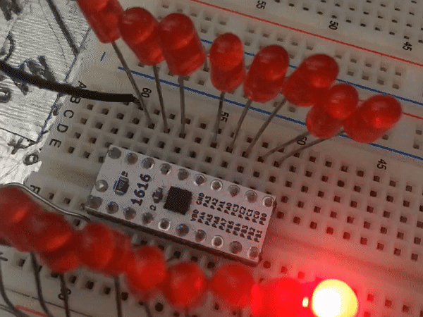
Testing the digital I/O set in Arduino can be done with a simple program and some LED’s on the output pins.
byte numPins=17;

void setup() {
  for (int i = 0; i <= numPins; i++) {
    pinMode(i, OUTPUT);
    digitalWrite(i, HIGH);
  }
}

void loop() {
  for (int i = 0; i <= numPins; i++) {
      digitalWrite(i, LOW);
      delay(50);
      digitalWrite(i, HIGH);
  }
}
Results in:
PORTMUX is next!
Discussions
Become a Hackaday.io Member
Create an account to leave a comment. Already have an account? Log In.
Great, I just found out that the original AVR was storing PORT and pin in the flash memory, just as described above. So the concept with the arrays for the new 0- and 1-series is not new, it was just moved from the pins_arduino.c in the core to the pin_arduino.h in the variant folder. Keeping all this data in the header files makes sense to me.
Are you sure? yes | no
Great work to show people how to do this, thanks!
Are you sure? yes | no
Really nice work and write-up! Love the effort you put into this and would love to give you a "like" for every post :)
Are you sure? yes | no