 Sander van de Bor
A new feature, not seen on the ATtiny series before, is Configurable Custom Logic (CCL). CCL allows you to combine some inputs to create an output that runs totally independent of the MCU. Using this option can eliminate the need of flip-flops to control some basic operations.
The simplest examples of using CCL is by using the I/O pins. Dedicated inputs can be combined to trigger predefined output pins. See below diagram of the ATtiny1616 with the CCL pins in yellow:
Up to 3 different inputs can be combined to trigger an output. Above you can see PA0, PA1 and PA2 can be used as inputs for CCL0 to control the output on PA4. A good example can be found here:
Input pins is not the only input source for the CCL, but the following options are available as well:
- Events
- Analog comparator
- Timers
- Serial communication like USART and SPI
- Output from LUT (from other CCL)
See a complete overview on page#452 of the ATtiny1616 datasheet.
Atmel Start has a great example of using timers with CCL to control an LED on the output pin. Unfortunately, I had a hard time understanding the code and the code would not work out of the box within the Arduino ATtiny core. This log will describe the “Realistic Heartbeat tiny817” example from Atmel Start and how this can be used on the ATtiny1616 which is compiled with Arduino.
Getting started
The original code can be found on Atmel Start:
https://start.atmel.com/#examples/realistic/heartbeattiny817
Just search for “Realistic Heartbeat tiny817” and open the selected example. Tabs on the left will give you the options to get a flow-chart of the timers and CCL used. You can download the code and use Atmel Studio to execute the code. Using the same code in Arduino will not work since some of the timers are configured differently.
The “Realistic Heartbeat” example uses two timers to create a pulsing output on the CCL output pin which can be shown with an LED. In this case we are going to use CCL1 and that output is on PA7 (see diagram above).
The first timer is used to create the two pulses for the heartbeat where the second pulse is slightly stronger and longer, just like a real heartbeat. TCD0 in One Ramp Mode is excellent to create these two pulses since it allows two different compare values on a single cycle. See page#273 of the ATtiny1616 datasheet for more information. Compare value A can be used to create an output on WOA, while value B is used for WOB.
The ATtiny Arduino core is using Dual Slope Mode to control the PWM output pins PC0 and PC1. Changing the TCD0 back to One Ramp Mode is done as follows:
TCD0.CTRLB = 0x00; /* Disable Dual slope mode */
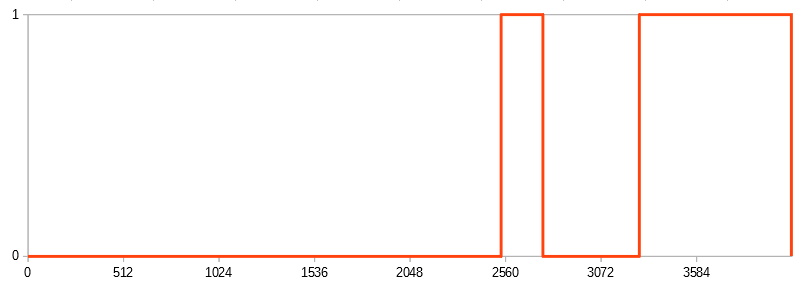
For the two pulses we have to define a duration. The TCD0 timer is 12 bits, so we create two pulses between 0 to 4095. The first pulse starts at 2536 and ends at 2760 while the second starts at 3277 and ends at 4092. I will explain a little later why we cannot use 4095 to end the second pulse.
TCD0.CMPASET = 2536; /* Compare A Set: 2536 */
TCD0.CMPACLR = 2760; /* Compare A Clear: 2760 */
TCD0.CMPBSET = 3277; /* Compare B Set: 3277 */
TCD0.CMPBCLR = 4092; /* Compare B Clear: 4092 */
After the second pulse ends (Compare B clear) the timer will start over again which will result in the following two pulses:
TCD0 uses the 20MHz and in this example we are using the counter prescaler with a division factor of 4:
while ((TCD0.STATUS & TCD_ENRDY_bm) == 0); /* Wait for Enable Ready to be high */
TCD0.CTRLA = 1 << TCD_ENABLE_bp     /* Enable: enabled */
  | TCD_CNTPRES_DIV4_gc;        /* Sync clock divided by 4 */
The total cycle can be calculated with the equation from page#272 of the ATtiny1616 datasheet: This cycle is too fast to notice the pulses with the naked eye, but we are going to use a second timer to visualize the pulse and create a fade in and out pattern.
The second timer will be TCB0. This timer is only 8 bits, counting from 0 to 255:
TCB0.CTRLB =  1 << TCB_CCMPEN_bp  /* Pin Output Enable: enabled */
  | TCB_CNTMODE_PWM8_gc;        /* 8-bit PWM */
The largest pre-scaler is only 2:
TCB0.CTRLA = TCB_CLKSEL_CLKDIV2_gc  /* CLK_PER/2 (From Prescaler) */
  | 1 << TCB_ENABLE_bp;       /* Enable: enabled */
And create a PWM output (40/255 =~ 16%) within this cycle as follows:
TCB0.CCMP = 0x28FF; /* 8-bit mode. Period = 255 (0xff), cmp = 40 (0x28) */
That small pre-scaler is a problem. The goal is to get a total cycle which is almost similar to the cycle time of TCD0. This can only be achieved by slowing down the Main Clock that is used by TCB0. Since we are not going to use any other code where the main clock is important it is possible to slow down the main clock in the setup of the sketch without setting any fuses. This will work when a bootloader is used as well since it will not slow down till the following code is executed:
_PROTECTED_WRITE(CLKCTRL_MCLKCTRLB, (CLKCTRL_PDIV_32X_gc | CLKCTRL_PEN_bm)); // Slow down the main clock to 20MHz/32 = 625kHz
Running the main clock at only 625kHz will result in the following cycle time for TCB0: It takes slightly longer for the TCB0 to complete a cycle resulting in the following sequence:
This entire process from beginning till end takes:
0.895Hz * 60 = 54BPM, a normal heartbeat while resting.
By using a slightly shorter cycle time for TCD0 this 54BPM sequence was created. If CMPBCLR was the maximum of 4095, then the two timers will have the same cycle time and will never overlap as shown below:
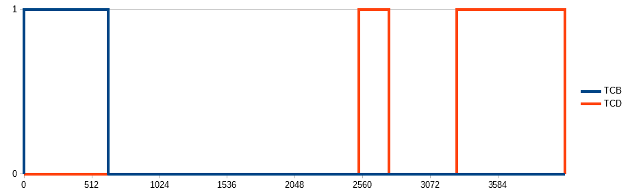
Graph of both timers running over time (~10x slower)
Looking at the sequence above we like to create an output when TCB0 and TCD0 are overlapping. We can use CCL to do so. First we assign the timer outputs (WOA and WOB for TCD0 and WO for TCB0) to the CCL1 inputs as follows:
CCL.LUT1CTRLB = CCL_INSEL0_TCD0_gc  /* TCD0 WOA input source */
  | CCL_INSEL1_TCD0_gc        /* TCD0 WOB input source */;
  CCL.LUT1CTRLC = CCL_INSEL2_TCB0_gc  /* TCB0 WO input source */;
Next, we complete the so-called CCL truth table. In this table different input resources are combined to determine when an output should be on.
| C TCB WO | B TCD WOB | A TCB WOA | OUTPUT PA7 |
| 0 | 0 | 0 | 1 |
| 0 | 0 | 1 | 1 |
| 0 | 1 | 0 | 1 |
| 0 | 1 | 1 | 1 |
| 1 | 0 | 0 | 1 |
| 1 | 0 | 1 | 0 |
| 1 | 1 | 0 | 0 |
| 1 | 1 | 1 | 1 |
We are pulling the LED to ground to turn it on and have the pin HIGH (1) to turn it off. For that reason, we only pull the output to ground when TCB and WOB are true, or when TCB and WOA are true. We could add the last condition, but since WOA and WOB are never true at the same time this will never create an output anyway. Reading from bottom to top we get 0b10011111 in the output. Converting that binary output to a hex value will result in 0x9F.
CCL.TRUTH1 = 0x9F; /* Truth 0: 0x9F */
Next we have to enable the look-up table and the use of the output for the LED:
CCL.LUT1CTRLA = 1 << CCL_ENABLE_bp  /* LUT Enable: enabled */
  | 1 << CCL_OUTEN_bp;        /* Output Enable: enabled */
And at the end we can start the CCL, and have the option to keep it running in standby as follows:
CCL.CTRLA = 1 << CCL_ENABLE_bp      /* Enable: enabled */
  | 0 << CCL_RUNSTDBY_bp;       /* Run in Standby: disabled */
That’s all! Connect an LED between PA7 and VCC and enjoy the heartbeat.
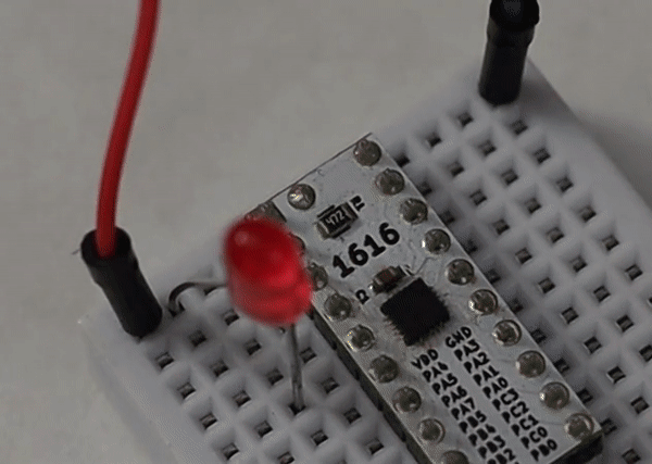
And yes, I did not use a current resistor on the LED ...
void TCB0_init(void)
{
  TCB0.CTRLA = TCB_CLKSEL_CLKDIV2_gc  /* CLK_PER/2 (From Prescaler) */
  | 1 << TCB_ENABLE_bp;               /* Enable: enabled */

  TCB0.CTRLB =  1 << TCB_CCMPEN_bp    /* Pin Output Enable: enabled */
  | TCB_CNTMODE_PWM8_gc;              /* 8-bit PWM */

  TCB0.CCMP = 0x28FF;                 /* 8-bit mode. Period = 255 (0xff), cmp = 40 (0x28) */
}

void TCD0_init(void)
{
  TCD0.CTRLB = 0x00;                  /* Disable Dual slope mode */

  TCD0.CMPASET = 2536;                /* Compare A Set: 2536 */
  TCD0.CMPACLR = 2760;                /* Compare A Clear: 2760 */
  TCD0.CMPBSET = 3277;                /* Compare B Set: 3277 */
  TCD0.CMPBCLR = 4092;                /* Compare B Clear: 4092 */

  while ((TCD0.STATUS & TCD_ENRDY_bm) == 0); /* Wait for Enable Ready to be high */

  TCD0.CTRLA = 1 << TCD_ENABLE_bp     /* Enable: enabled */
  | TCD_CNTPRES_DIV4_gc;              /* Sync clock divided by 4 */
}

void CCL_init(void)
{
  CCL.LUT1CTRLB = CCL_INSEL0_TCD0_gc  /* TCD0 WOA input source */
  | CCL_INSEL1_TCD0_gc                /* TCD0 WOB input source */;

  CCL.LUT1CTRLC = CCL_INSEL2_TCB0_gc  /* TCB0 WO input source */;

  CCL.TRUTH1 = 0x9F;                  /* Truth 0: 0x9F */

  CCL.LUT1CTRLA = 1 << CCL_ENABLE_bp  /* LUT Enable: enabled */
  | 1 << CCL_OUTEN_bp;                /* Output Enable: enabled */

  CCL.CTRLA = 1 << CCL_ENABLE_bp      /* Enable: enabled */
  | 0 << CCL_RUNSTDBY_bp;             /* Run in Standby: disabled */
}

void setup()
{
  _PROTECTED_WRITE(CLKCTRL_MCLKCTRLB, (CLKCTRL_PDIV_32X_gc | CLKCTRL_PEN_bm));  /* Slow down the main clock to 20MHz/32 = 625kHz */

  TCB0_init();
  TCD0_init();
  CCL_init();
}

void loop() {
    /* Nothing to do here */
}
Discussions
Become a Hackaday.io Member
Create an account to leave a comment. Already have an account? Log In.