0%
0%
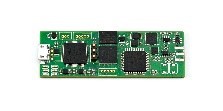
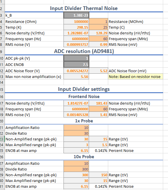
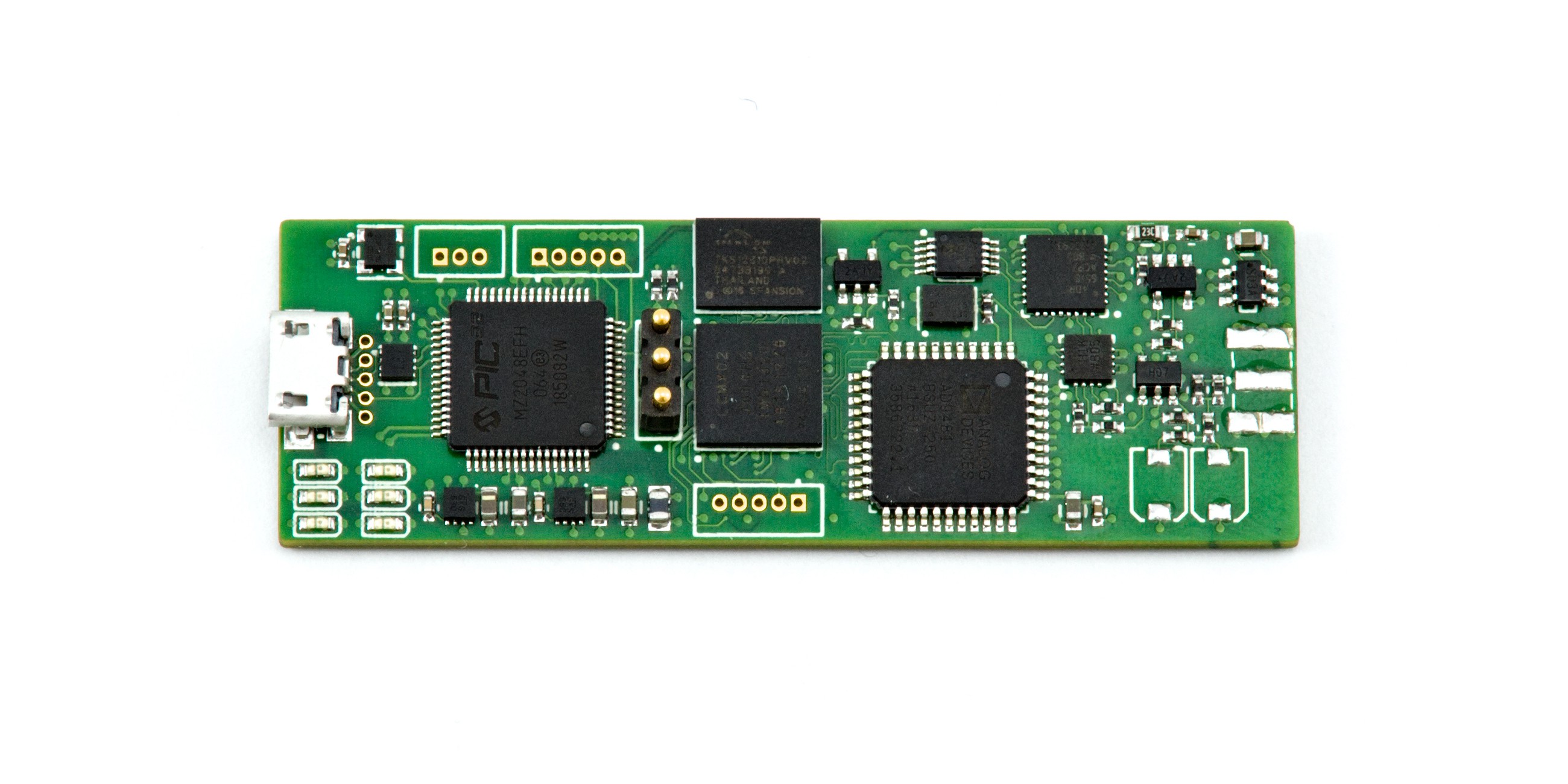
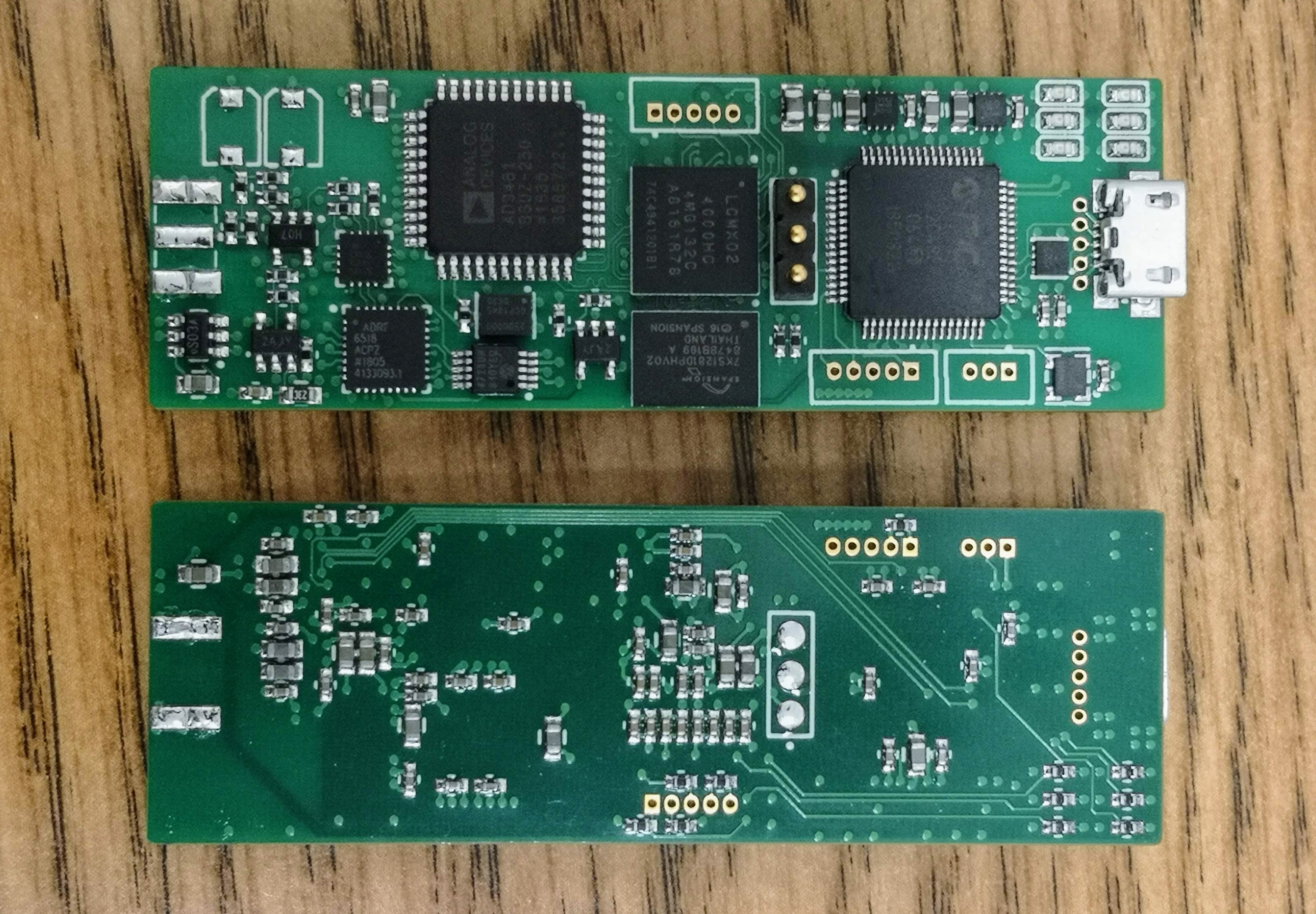
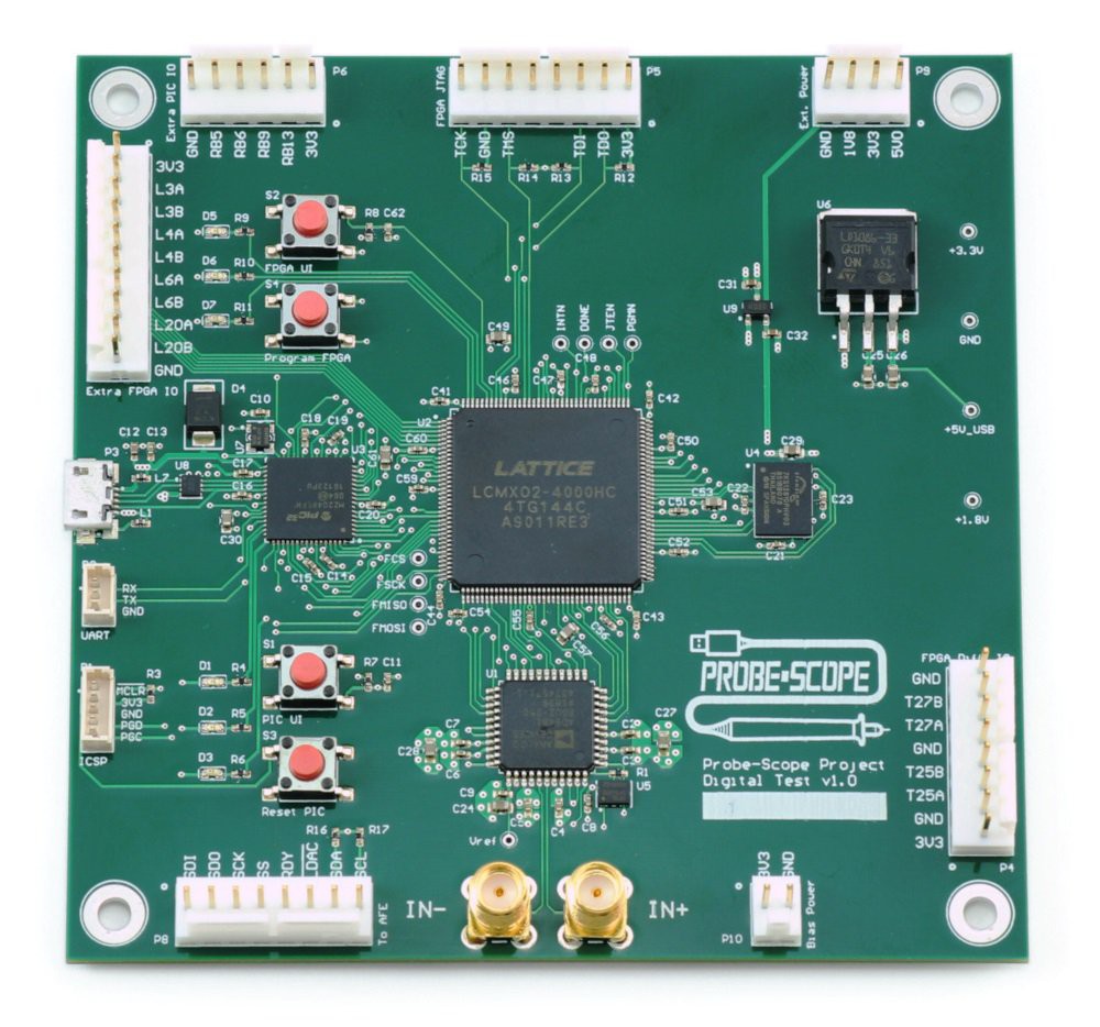
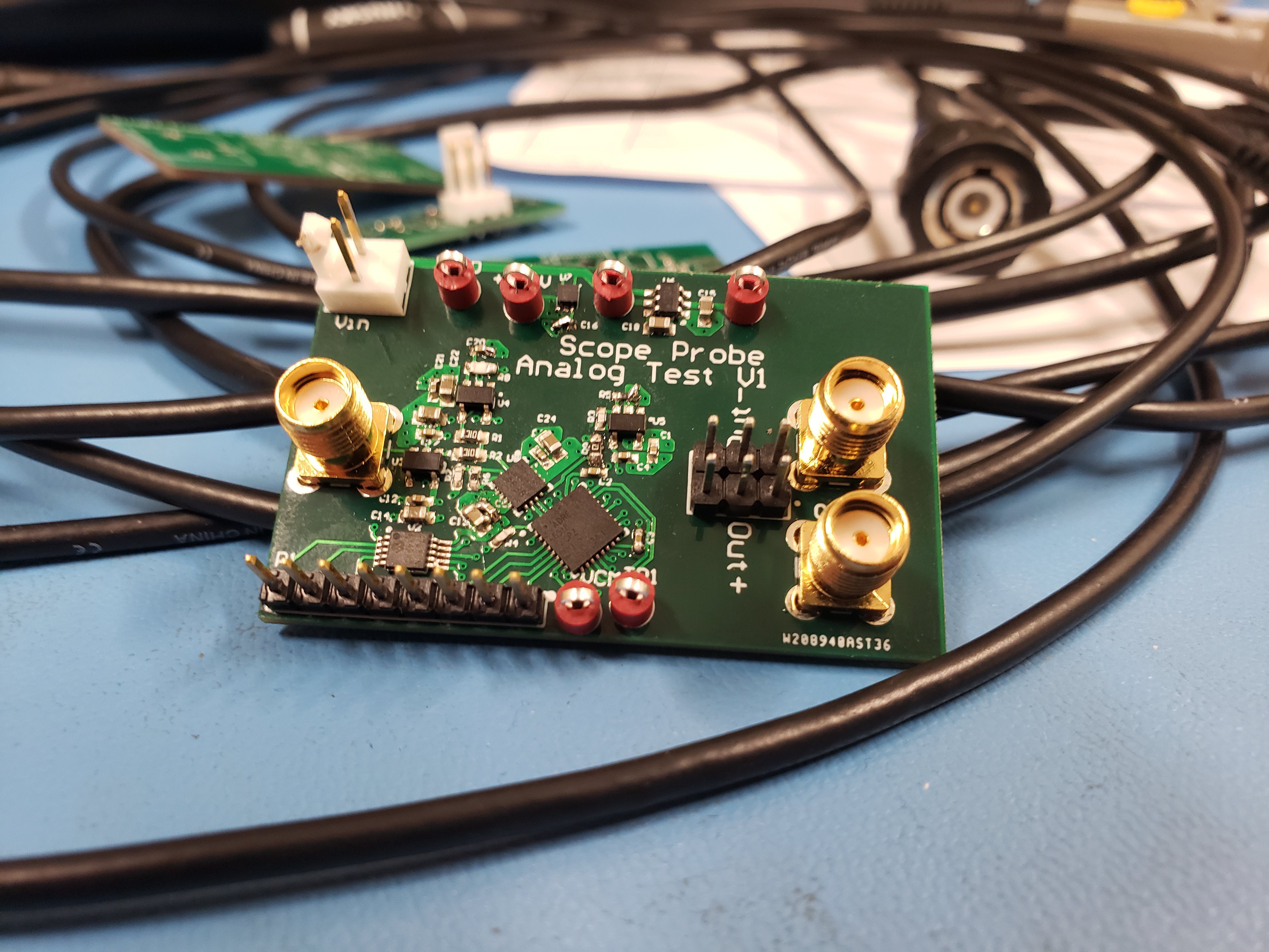
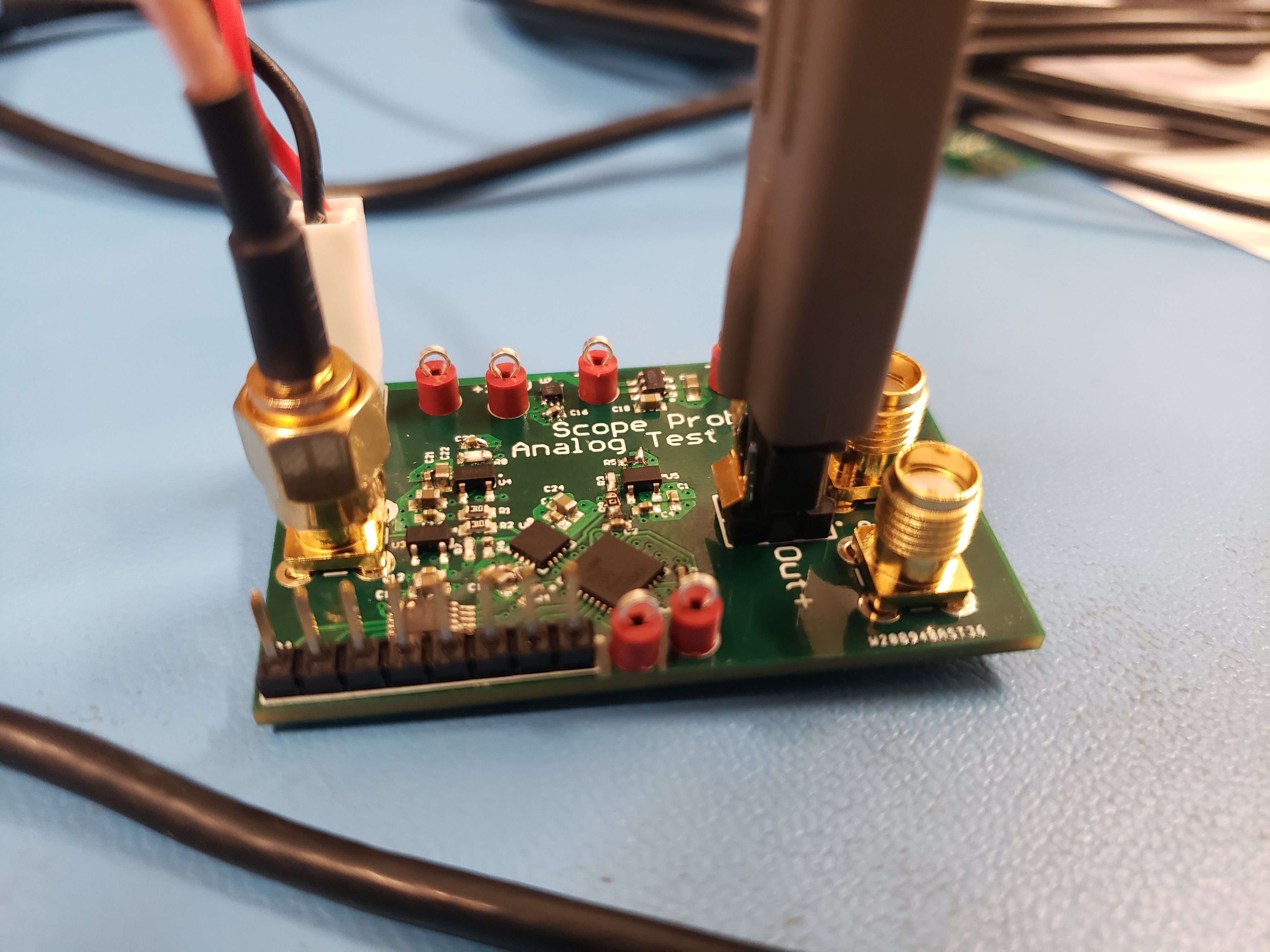
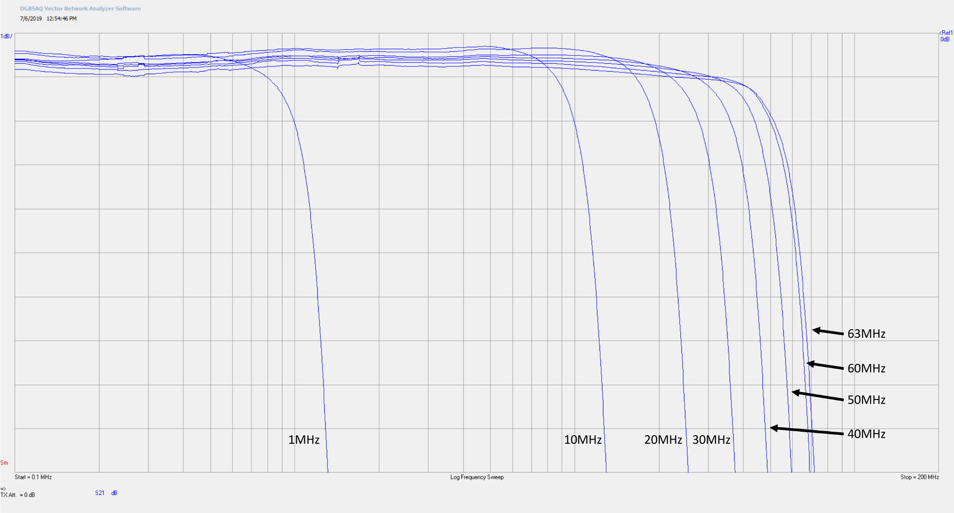
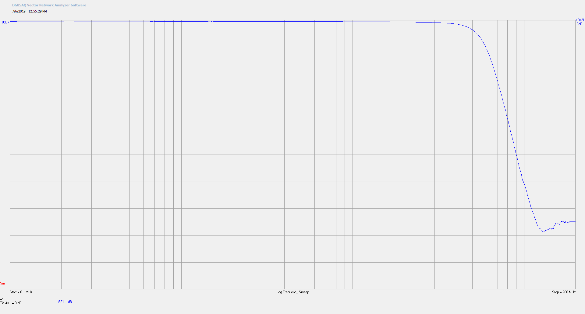
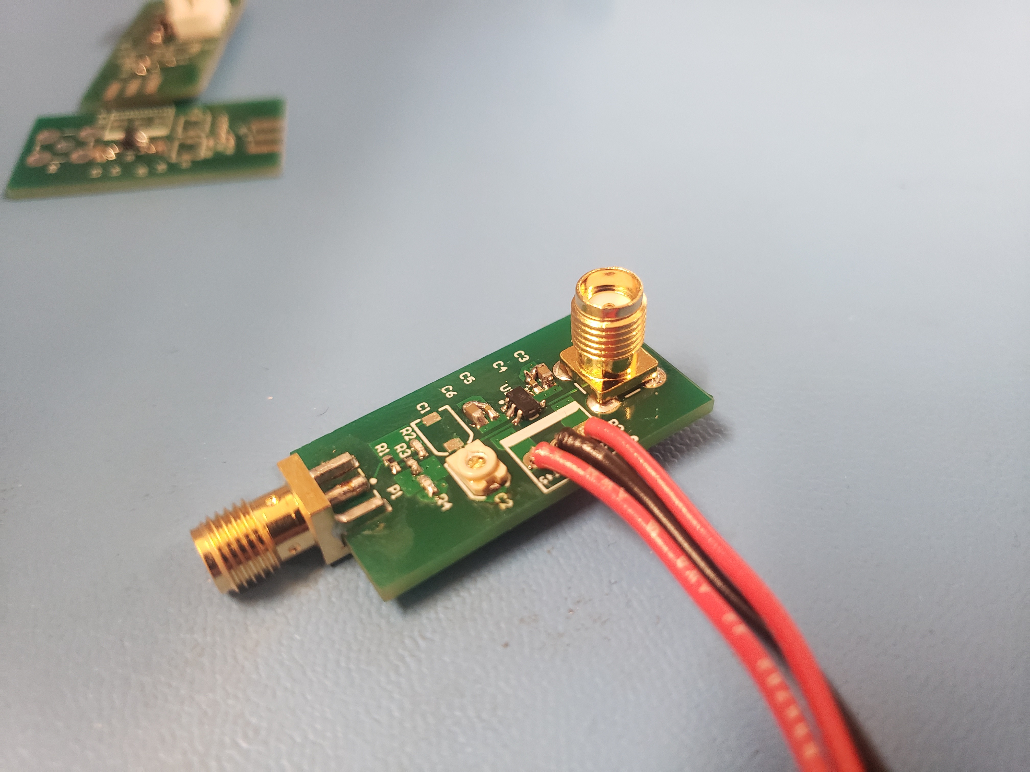
60MHz Bandwidth 250Msps Probe-Scope
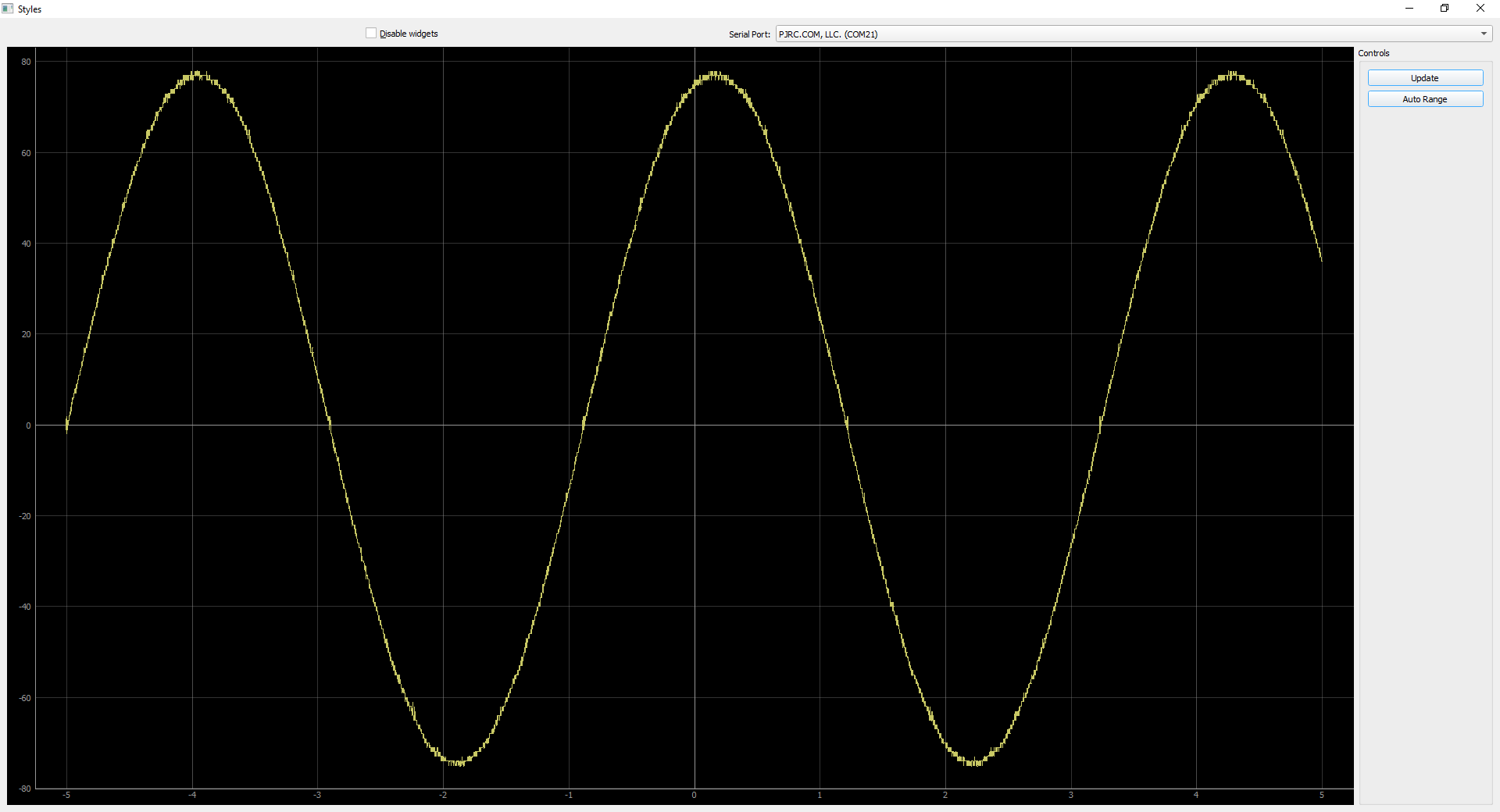
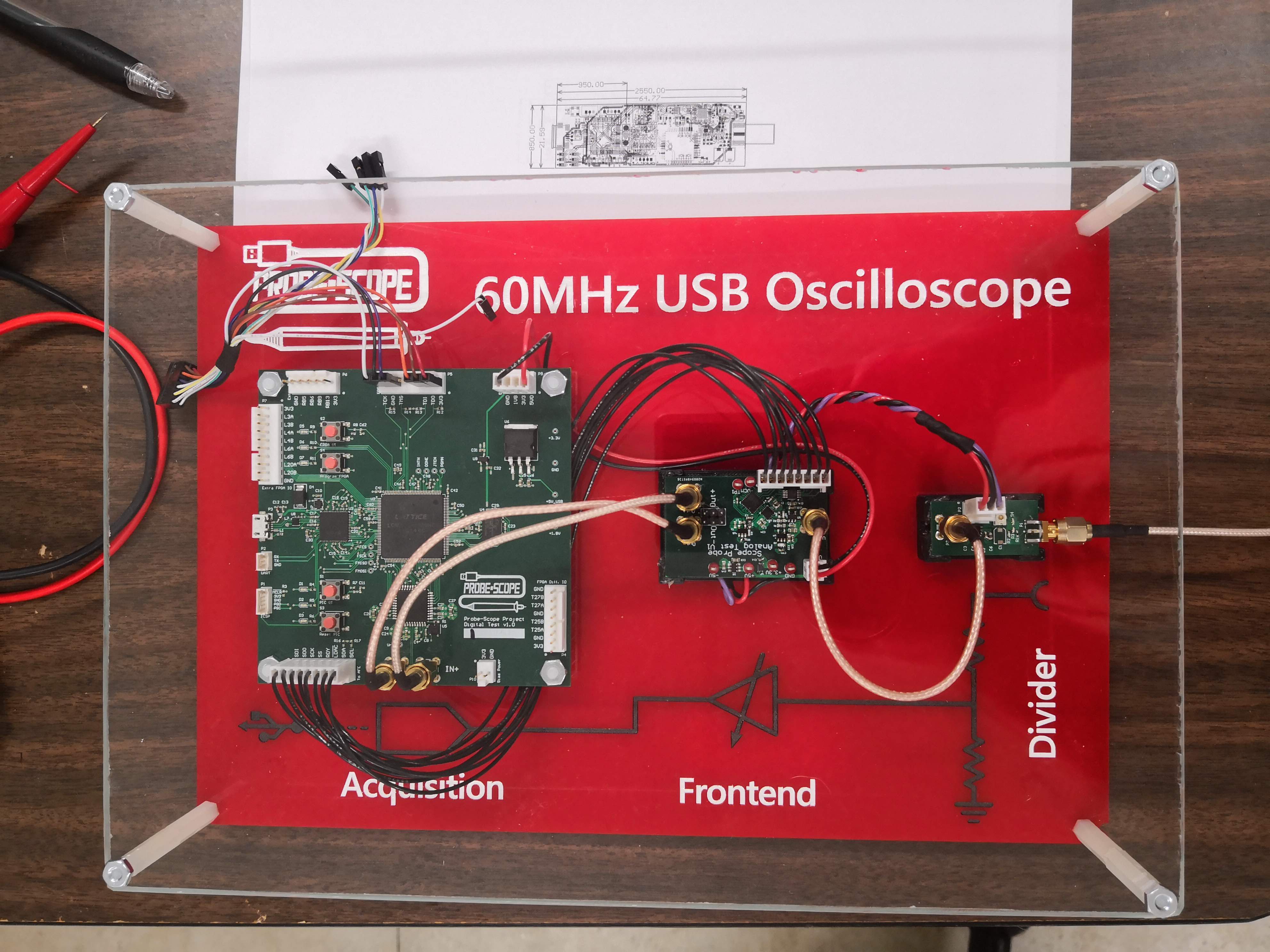
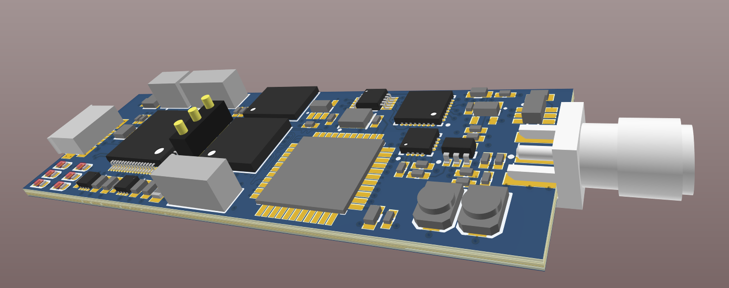
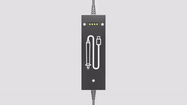
The Probe-Scope is an open source 60MHz 250Msps oscilloscope probe with all guts built right in, that plugs directly into your PC via USB
 Mark Omo
Become a Hackaday.io member
Already have an account? Log in.
Just one more thing
To make the experience fit your profile, pick a username and tell us what interests you.
Pick an awesome username
hackaday.io/
Your profile's URL: hackaday.io/username. Max 25 alphanumeric characters.
Pick a few interests
Projects that share your interests
People that share your interests


 Jon Klein
 Jonas Norling
 Luke Valenty
 Clyne
Clyne
Is this project still being developed. Im really interrested since it would be incredible for field work but as the PC software is...quite primitive Im not really convinced. If you decide to develop the software further or maybe even get integration into some other software like Pulseview by Sigrok or a different ready made software