 James Rowley
In a similar fashion to the Analog Input Test Board, we created a Digital Test Board, so that we could compartmentalize development efforts and get both halves of our system up and running at the same time. The Digital Test Board contains the Analog Devices AD9481 ADC and everything needed to get data out of it and on to a computer over USB: to accomplish this it uses a Lattice MachXO2-4000 FPGA, a Cypress S70KS1281 self-refreshing DRAM, and a Microchip PIC32MZ2048EFH MIPS microcontroller.
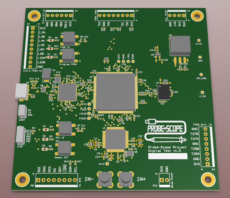
The ADC is clocked by a Microchip DSC1103 250MHz LVDS MEMS oscillator, and since its output is 250Msps Double Data Rate (DDR), its output clock is 125MHz. It has two output ports, A and B, each 8 bits, with A being valid on the falling edge of the clock and B on the rising edge. The data clock output from the ADC is used as the clock source for the FPGA, which has built-in DDR support on the bottom IO cells.
Once the data gets into the FPGA, it’s stored into “EBR” SRAM in FIFO mode (a hardened feature of the MachXO2), where it waits until it can get send out in blocks to the Cypress “HyperRAM” device. Also at this time, the FPGA checks the incoming data for a trigger condition. We use the FPGA’s PLL to generate a 166MHz clock for the HyperRAM, which is its top speed. Since the HyperRAM is a self-refreshing DRAM, it does have to spend some time refreshing occasionally, and we also have to reset the address when we get to the end of the memory, so we can’t just write continuously at the ADC’s output frequency. Instead we run it slightly faster and write out bursts of data, allowing for control and refreshing to occur in between bursts.
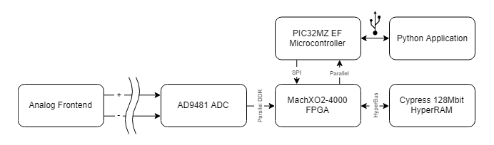
The PIC controls the FPGA via SPI (using the FPGA’s hardened SPI peripheral) and also with simple GPIO. It sets the trigger conditions for the FPGA, and when a trigger is detected, it requests the relevant slice of data from the FPGA, which will transfer it out of the HyperRAM and into the PIC via a parallel port. At the same time (since in most circumstances the PIC cannot hold all the data at once), the PIC transfers the sample data over USB to a Python application running on the user’s computer. The design data for the digital test board can be found on our GitHub, and here is a direct link to the PDF:
Our boards have finally been shipped, so we'll get them hopefully on Wednesday and build them this week.
Discussions
Become a Hackaday.io Member
Create an account to leave a comment. Already have an account? Log In.