 James Rowley
We recently got our PCBs in and built up, and having detailed the testing of the analog boards, it’s time to show off the Digital Test Board in its early stages. Unlike the analog boards, where the bulk of the work was done in designing them before they were made, this was straightforward to design and will take much more effort to program. So, expect some more updates over the weeks as all the software and firmware gets put together.
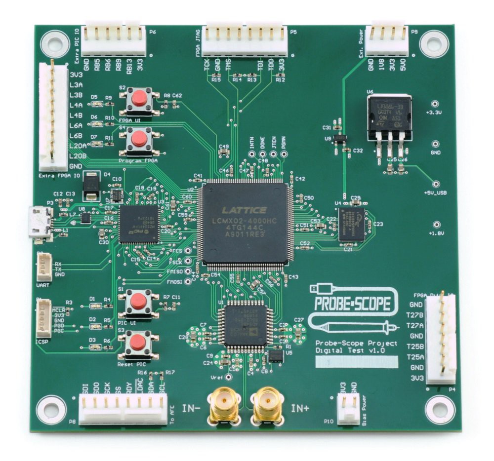
First, a glamour shot:
We need to get the final Probe-Scope board designed and sent out fairly soon, since the lead times for getting it made and assembled (and we will be getting it assembled) are pretty long due to the high density, and the competition deadline is approaching. So, to start off, we’re just verifying that all the pieces of the digital test board work so that we can be comfortable reusing those schematics in the final design. That means probing the ADC to make sure it’s outputting data (it is), loading code onto the PIC and FPGA to make sure they run with the correct clock sources, and then eventually (not done yet but soon) implementing a simple USB device on the PIC, and operating the HyperRAM with the FPGA.
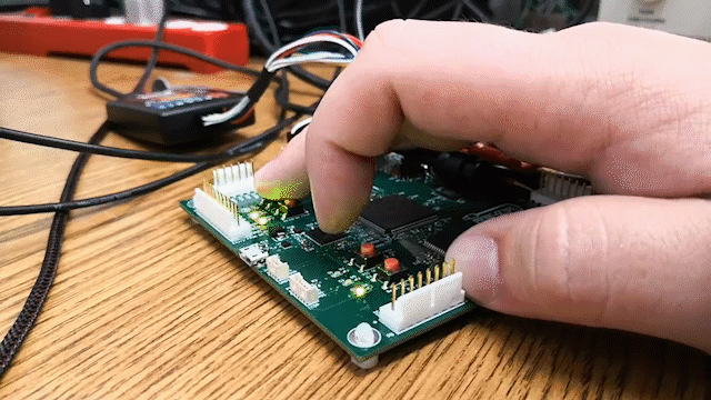
The PIC was easy to get running as we have some lightweight test code we often reuse, and it works just fine with the external 24MHz oscillator (which is basically required for USB to work). The FPGA, on the other hand, was a bit more of a challenge for me as I have not used Lattice Diamond before, and its documentation is very spread out. Pro-tip: the file list has tabs at the bottom… you really want to check out the process tab. At any rate, I got that running too, clocked off the output of the ADC. Watch it all blink:
This leaves the USB and the RAM to be tested. The USB connections and clock, I’m not too worried about, they match known good designs. The RAM however, I’m also not too worried about, but it remains to be proven that our concept of clocking it at a higher speed using the FPGA’s PLL will work in this exact configuration. Stay tuned…
EDIT: The PLL for the RAM worked perfectly fine, thanks to the configurator it wasn't a pain at all.
Discussions
Become a Hackaday.io Member
Create an account to leave a comment. Already have an account? Log In.