0%
0%
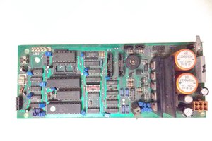
Dreamwriter 200 - Z80 Laptop
What can we do with a AIO Z80 laptop? Let's find out!
 Trevor Johansen Aase
Become a Hackaday.io member
Already have an account? Log in.
Just one more thing
To make the experience fit your profile, pick a username and tell us what interests you.
Pick an awesome username
hackaday.io/
Your profile's URL: hackaday.io/username. Max 25 alphanumeric characters.
Pick a few interests
Projects that share your interests
People that share your interests
 Ken Yap
 Marsupilami
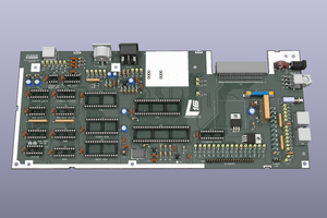
 SukkoPera
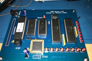
 Michael Cullen