 Brandon Reinhart
Today I hooked up the control logic for the A and B registers. The first step was to work out the wiring schematic on paper. Each register consists of two chips a 74HC245 bidirectional bus transceiver and a 74HC574 8 bit flip-flop. I want to be able to have three states for the register:
- Disabled - Low-impedance, the register isn't visible to the bus.
- Enabled - The register drives the bus lines.
- Load - The register latches the bus lines on a rising clock edge.
The register has four inputs to manage:
- 245::~OE - When high, the chip is in a low-impedance state. When low, output is enabled.
- 245::DIR - When low, the register side is output and the bus side is input. When high, the bus side is output.
- 574::~OE - When high, we latch if the CLK line is high. When low, output is enabled.
- 574::CLK - When high, we latch if output is disabled.
On the A and B registers, the control logic to drive these input lines are a Lx (latch) and Ex (enable) signal. We can break this into a state table that describes what the input lines should be to satisfy the signal:
- Ex
- Goal is to output the register's value to the bus.
- 245, ~OE=L, DIR=H
- 574, ~OE-L, CLK=X
- Lx
- Goal is to latch the bus to the register.
- 245, ~OE=L, DIR=L
- 574, ~OE=H, CLK=H
- Xx
- When the register is not loading or enabled we want to be in a low-impedance state.
- 245, ~OE=H, DIR=X
- 574, ~OE=H, CLK=L
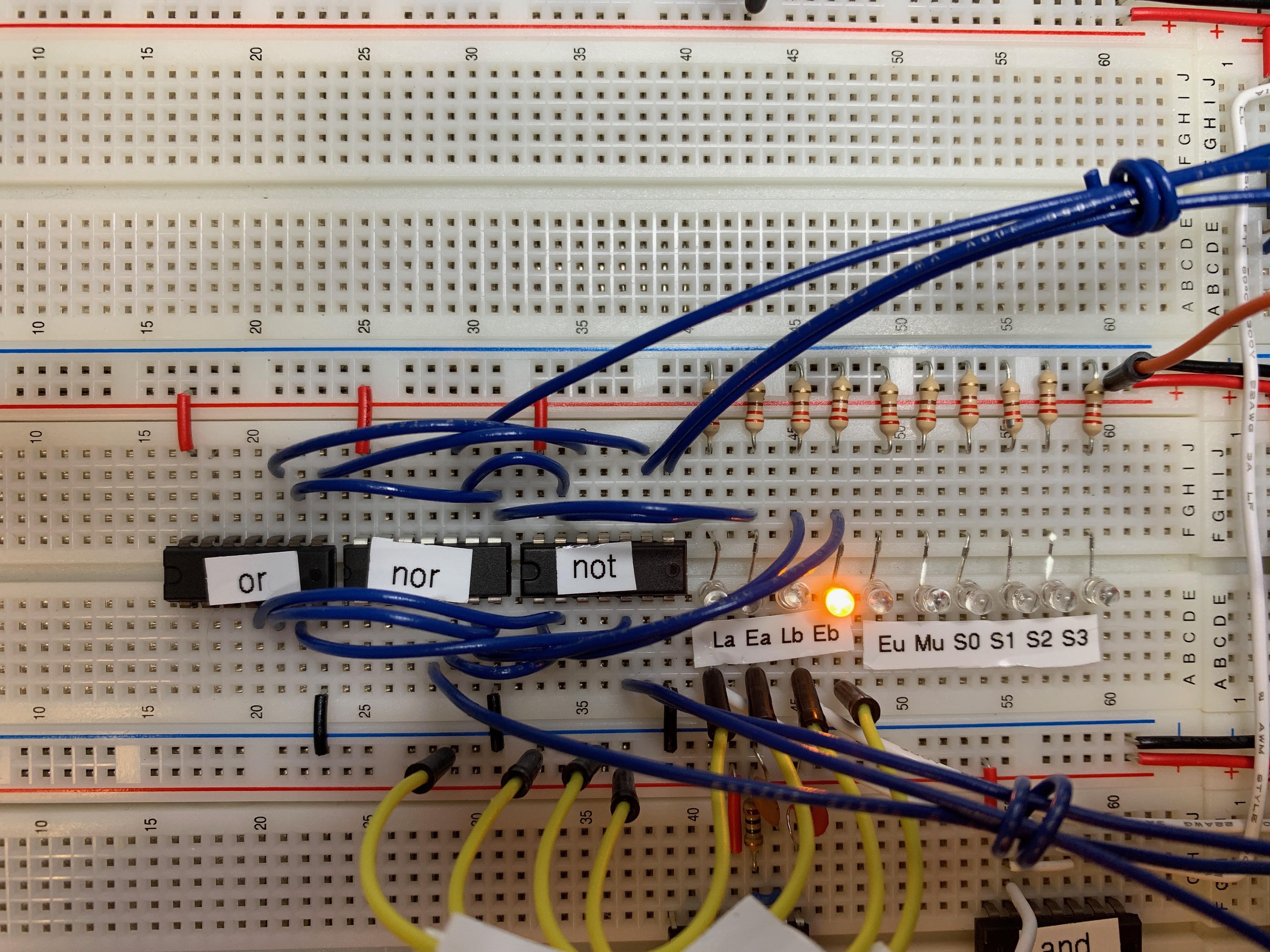
Once we have a mapping of our logic to our chip input lines, we can create a truth table to determine the logic we want to use to actually wire up the signals. In my case I didn't want to use more than 2 gates per chip. I use quad gate array chips, so 1 chip can support 2 registers. I like to write the logic out as a phrase that matches the state table above.
- 245::~OE = Ex nor Lx -- "high, unless E or L"
- 245::DIR = E or not L -- "high if E, low if L"
- 574::~OE = L or not E -- "high if L, low if E" -- which can be wired as nor( E or not L )
- 574::CLK = CLKs and L -- "high if L and system is clocked"
We combine the system clock with L to create the input clock, so that we are only clocking the flip-flop chip when we want to load something. We can also save some wires by using a nor gate to create the 574 output enable signal, since it lets us avoid having to not E.
I did all of this on paper:
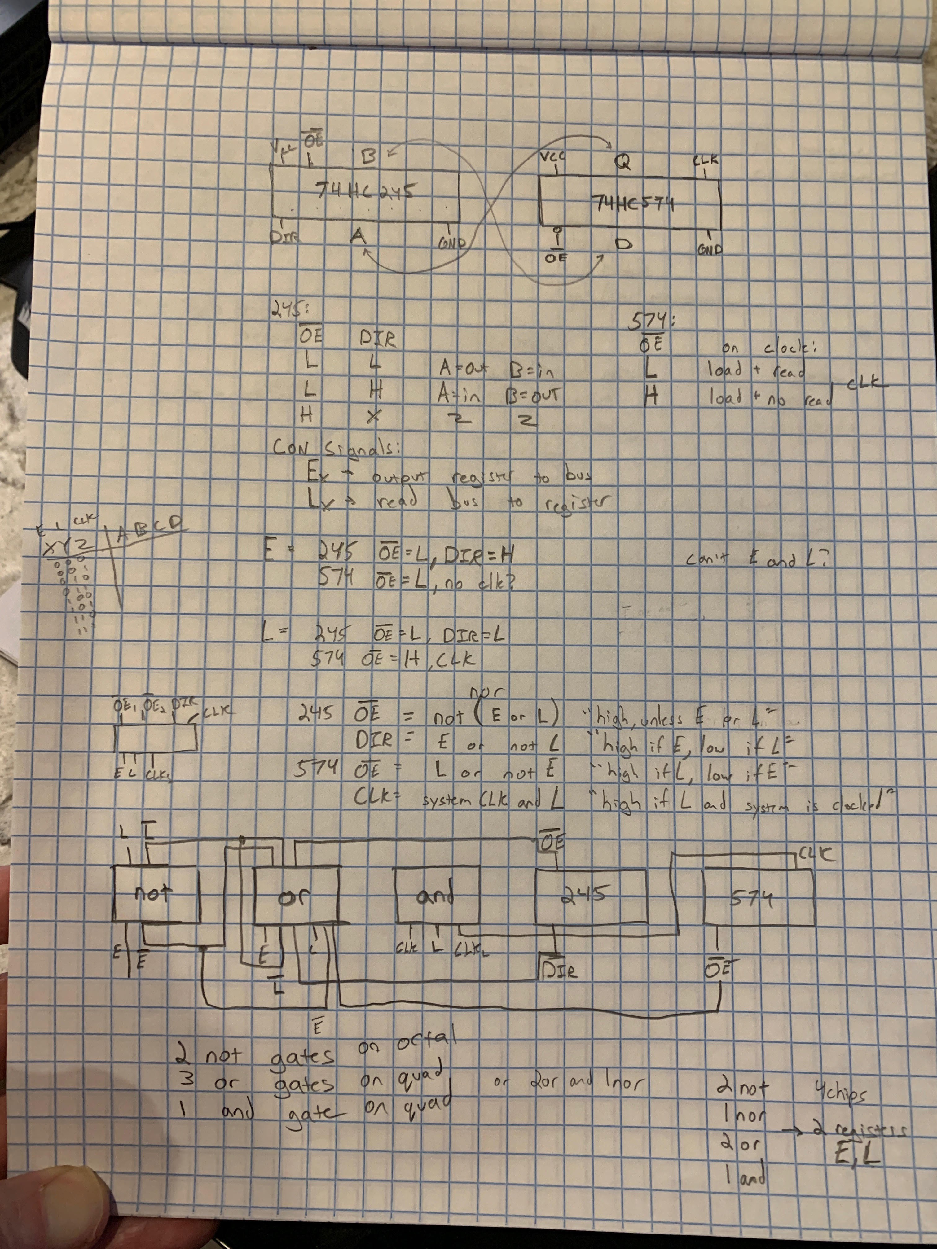
I just enjoy working out the logic on paper to be absolutely sure the schematic makes sense. The above doesn't show the nor gates which I added afterwards when I realized it simplified things a bit. There are probably other simplifications that I didn't find or didn't look for. I ended up using 1 NOT, 2 NOR, 1 OR, and 1 AND gate per register.
Another aspect of this approach is that the on state for a signal is high. This just keeps it simpler in my head, instead of having to worry about remembering something like "bit X of the CON word is not-L" because I wanted to save a NOT gate.
Here is the resulting CON wiring for the A and B registers:
The CLK and is done on the breadboard below, where I moved the clock circuit. I'll probably neaten up the lines by cutting them to the same height off the board before I implement another register's CON.
And here is the logic working. I previously latched a value into the B register and then I enabled that register to drive the bus:
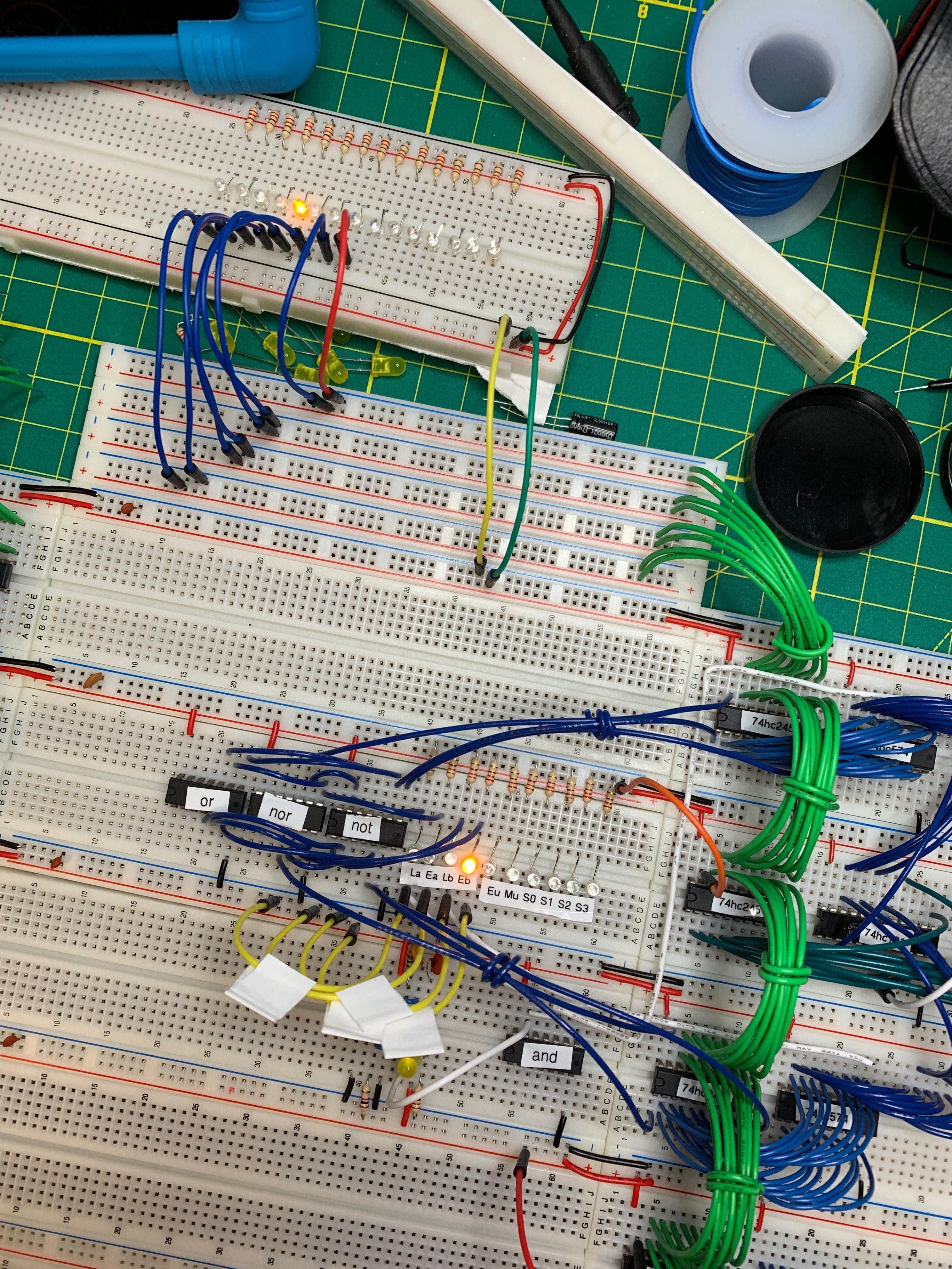
Another bank of of these chips will be placed below for the X and Y index registers and then each should also have enough gates free to drive the registers on the left side of the computer. The X and Y index registers will also have INC and DEC control lines.
So next up is a clean-up pass on the wiring, then wiring up all the other registers (as well as the ALU enable line) this same way.
The idiot lights really don't need to be there, but make debugging a lot quicker. I may pull them?
Discussions
Become a Hackaday.io Member
Create an account to leave a comment. Already have an account? Log In.