 Peter Wasilewski
Hello!
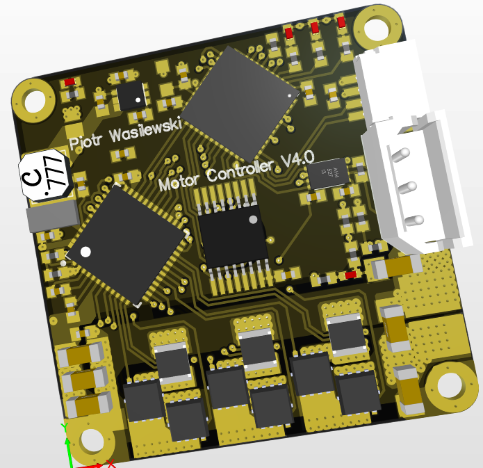
This time I’d like to focus on the new design of my brushless motor controller. The previous one, although it worked, had a lot of drawbacks. In this revision, I wanted to fix all the issues that were found in the first prototype:
-fix the shunt sensing paths - obligatory kelvin connections
-DRV8232RS (with internal buck converter) instead of DRV8323S - in order to power the device from the DC bus.
-use ceramic capacitors for DC bus.
-use FDCAN transceiver
-use the latest STM32G431 microcontroller as it has many hardware features supporting motor control and FDCAN peripheral
-reduce the size and make it rectangular for easier mounting
-single side component placement on a 4 layer board, hopefully with semi-automatic soldering using a stencil, solder paste and a reflow oven.
I believe the design came out very well. The four layer board is 33x33mm with a height of about 3-4 mm (where the connectors are the highest points). There are a few good practices I stumbled upon on the Internet that I’d like to mention. I do not think they are crucial for the device to operate correctly, however, it is good to know a few basic rules for future reference.
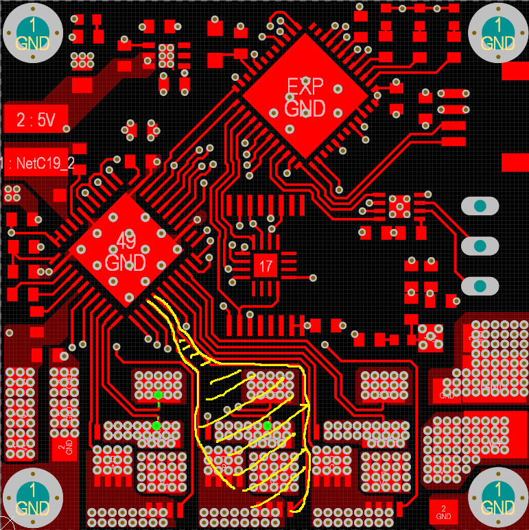
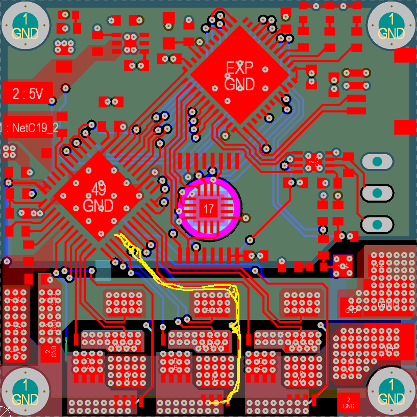
- Well designed, low inductance paths for charging and discharging the MOSFET gate’s capacitor. The loop formed by two connections: driver - MOSFET gate and driver - source of the transistor should be as small as possible. This may not influence the low frequency circuits, however when the frequency of switching rises (it’s really more about the fall and rise times of the drive signal) the loop’s inductance causes the current to rise more slowly and thus extending the time for the MOSFET to open completely. So the good practise is to keep these loops as small as possible. In the pictures below, you can see a comparison between a well-designed layout and a worse one with a big loop.
![]()
big loop example ![]()
small loop example - Separate the power and digital ground. This is something I kind of knew already. It is not recommended to push high currents under sensitive parts such as microcontrollers. So, in order, to prevent any kind of disturbance in the digital part, I completely separated the planes, connecting them in a single point near the driver. As the driver can push relatively high currents, I decided to put the connection between grounds near it so it can sink current from nearby DC bus capacitors.
![]()
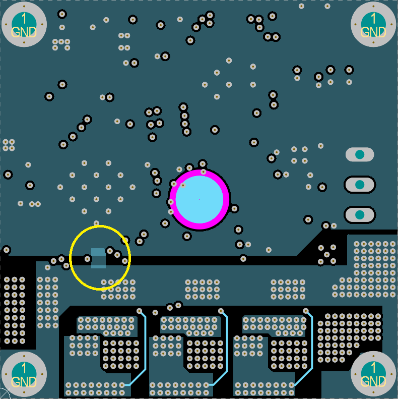
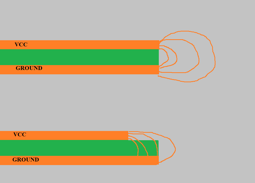
Separate ground connection - Ground in 4-layer board. However not crucial, it is a good practise to keep the ground layer directly under the component’s layer. Apparently it reduces the EMI generation, because the path to ground is as short as it can be. In this point I’d like to mention the VCC plane’s offset. Some sources say that you can lower the EMI on the edges of the board by offsetting the VCC plane in respect to the ground layer. I think the picture below explains it in a most simplified fashion.
![]()
EMI at the edge of a PCB - Via placement. It is quite controversial as there are many ways of putting a via near, for example, a bulk capacitor pads, that should be connected to inner VCC and GND layers. I decided for the lowest inductance option guided by the book by Levent Sevgi - “A Practical Guide to EMC Engineering”. I’m just a little worried about the soldering part. The vias placed partially on the pad can sink the solder and cause the component to stand up (tombstoning) or just not to solder correctly.
As I said earlier, above guidelines are considered good practices in designing a PCB layout, while not being crucial for basic circuits.
One thing I’m concerned about is the DC bus of the motor driver. Inspired by Benjamin Katz’s design and other small-size controllers I decided to use ceramic capacitors as well. Diving deeper in their specs I came across many characteristics of the capacitance vs dc bias voltage (https://community.cypress.com/docs/DOC-15088). A DC bias voltage can effectively lower the capacitance even to 20% of it’s initial value. What is more interesting the rate of capacitance change seems to be independent on the voltage rating. I will test the setup with ceramic capacitors, though I’ll keep in mind that there can be too little capacitance available on the DC bus.
In the above PCB pictures you can also see the double footprint for the encoder - I wanted to try out the less known ma702 encoder. Because of relatively high cost of the 4-layer PCB manufacturing, I made it compliant with both AS5xxx and MA7xx devices. New encoders are quite interesting as they cost less, are available in smaller packages, have similar resolution and can be placed near the shaft (side shaft placement) instead of axial placement.
Currently, I’m working on a small integrated actuator that will be used in the new robot. I want to make a standalone actuator that can be easily replaced or fixed. For this purpose I also started building my own, small sized CNC machine. My goal is to mill in aluminum so I can make durable housing for the actuators. Besides, I’m thinking about building a torque transducer for small sized motors. I would like to gather more data about the available power and cogging torque. Both parameters depend on the shaft position and thus cannot be measured on a regular stall torque test stand. If I had the dynamic torque sensor, I could determine if the controller is well designed or if it can be improved.
After over a month delay, the new PCB’s are on their way, so next time I’ll post some photos.
See you,
Peter.
Discussions
Become a Hackaday.io Member
Create an account to leave a comment. Already have an account? Log In.
Hi Peter, great design! I'm also designing a motor controller with similar application in mind. I'm wondering about the low-inductance path that you mentioned, have you seen noticeable effects of a bad vs. good design in the frequencies of 20-60kHz that are used in many hobby-grade motor controllers?
Are you sure? yes | no
Hi! Honestly I do not know, I havent received the PCBs yet. I'll try to make a comparison between the new design and the old one. However, if we consider the range of frequencies You mentioned, and the compact size of the PCBs, I don't think it's going to make a hudge difference.
Are you sure? yes | no
Looking forward to your results, and best of luck with the new board!
Are you sure? yes | no
Very nice design and so compact.
Are you sure? yes | no