0%
0%
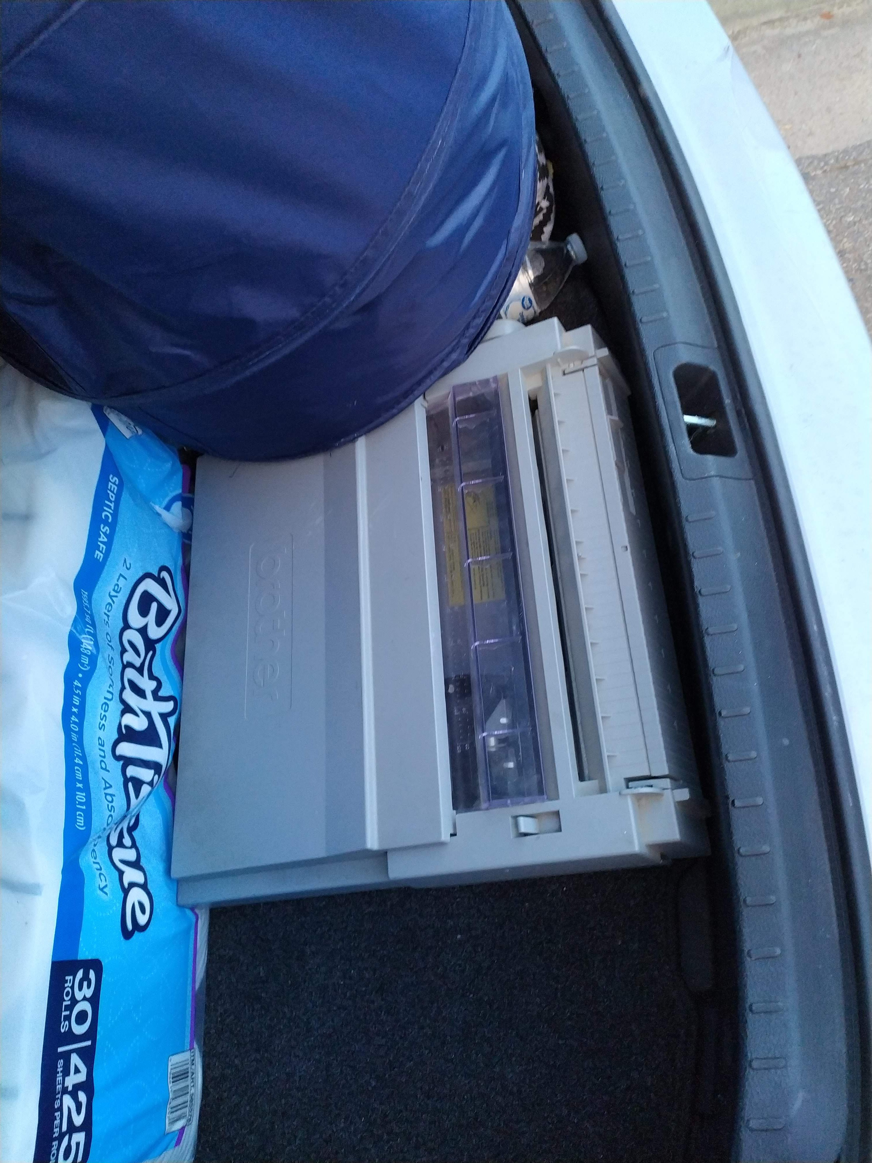
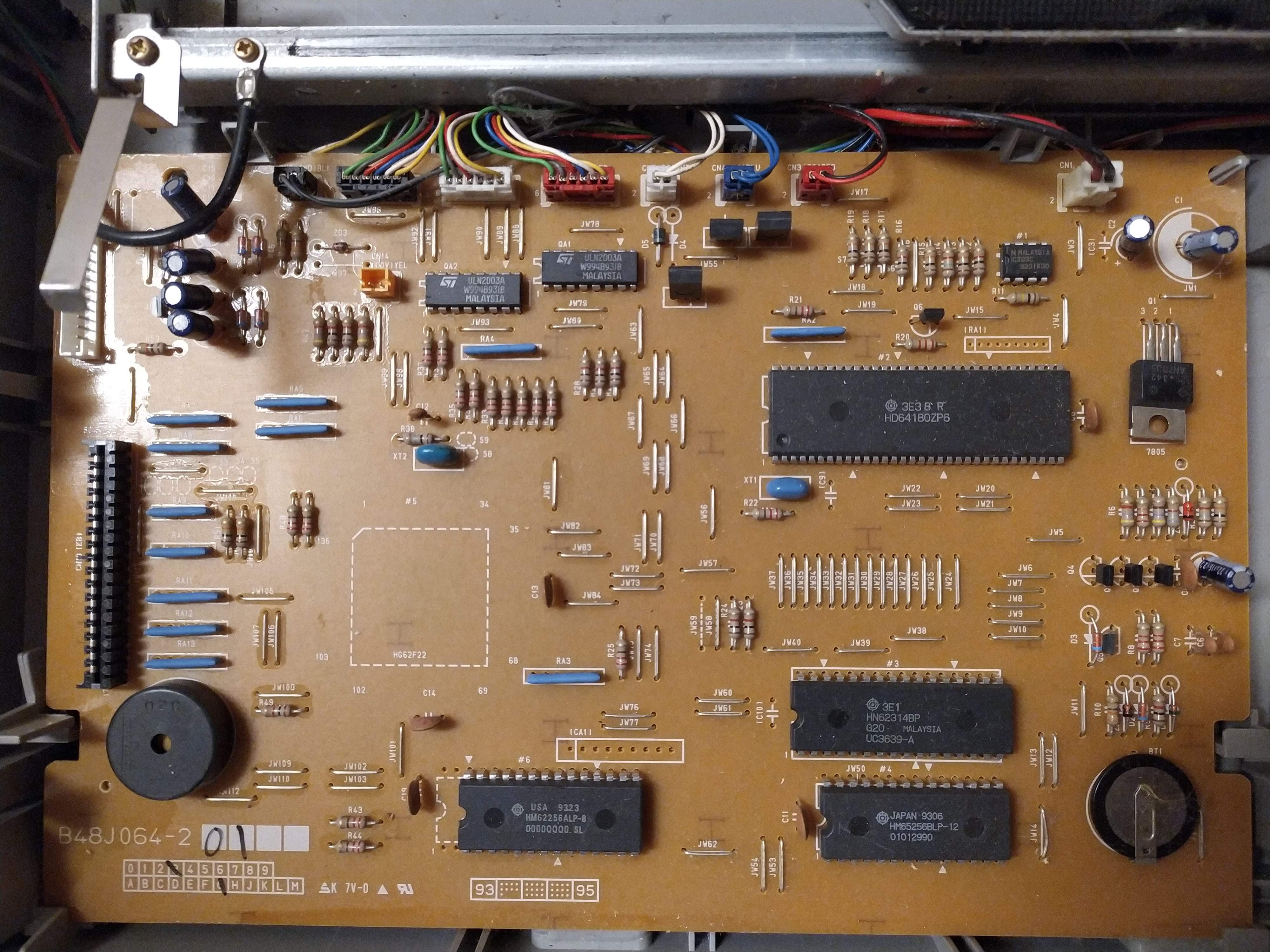
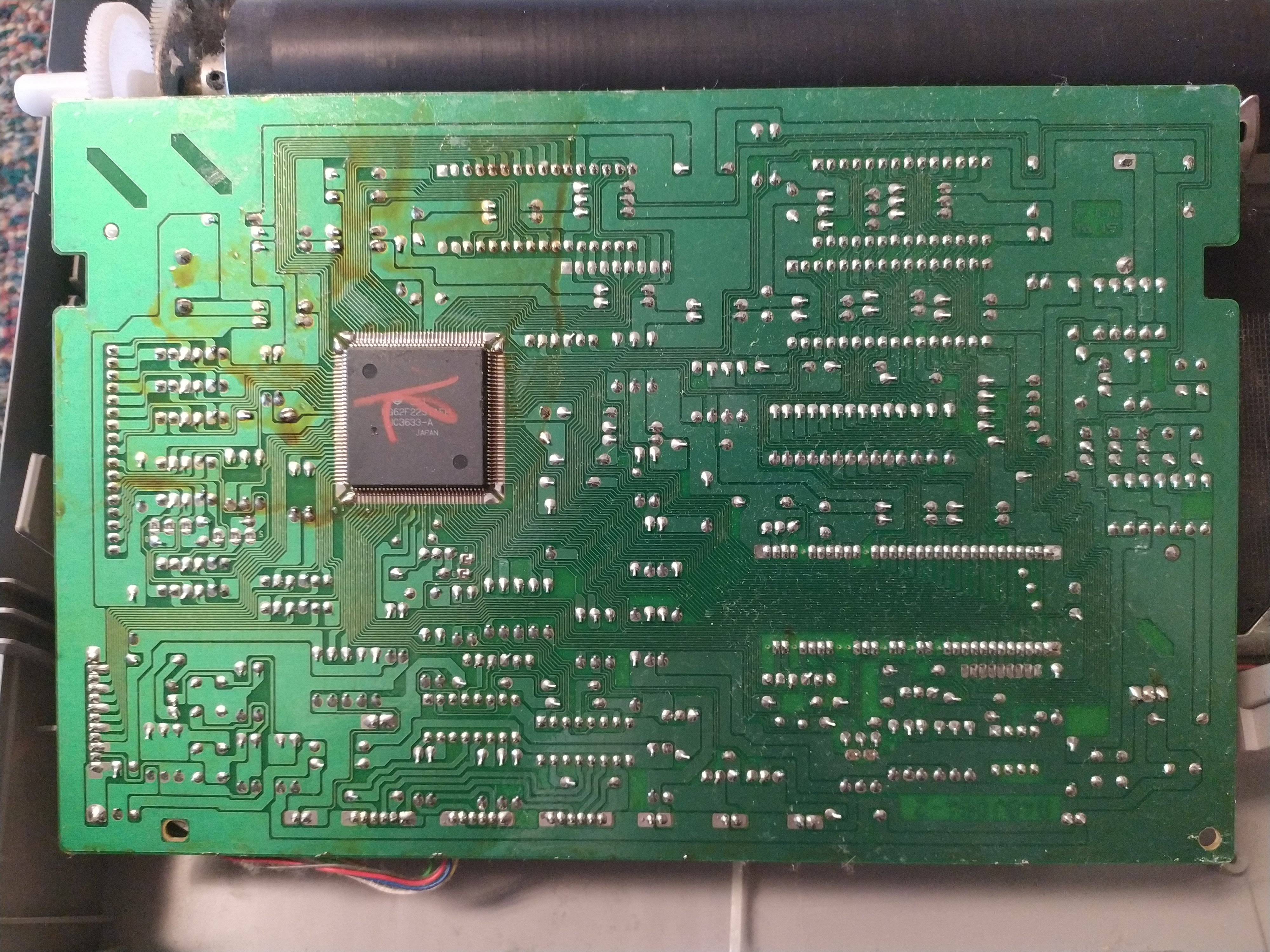
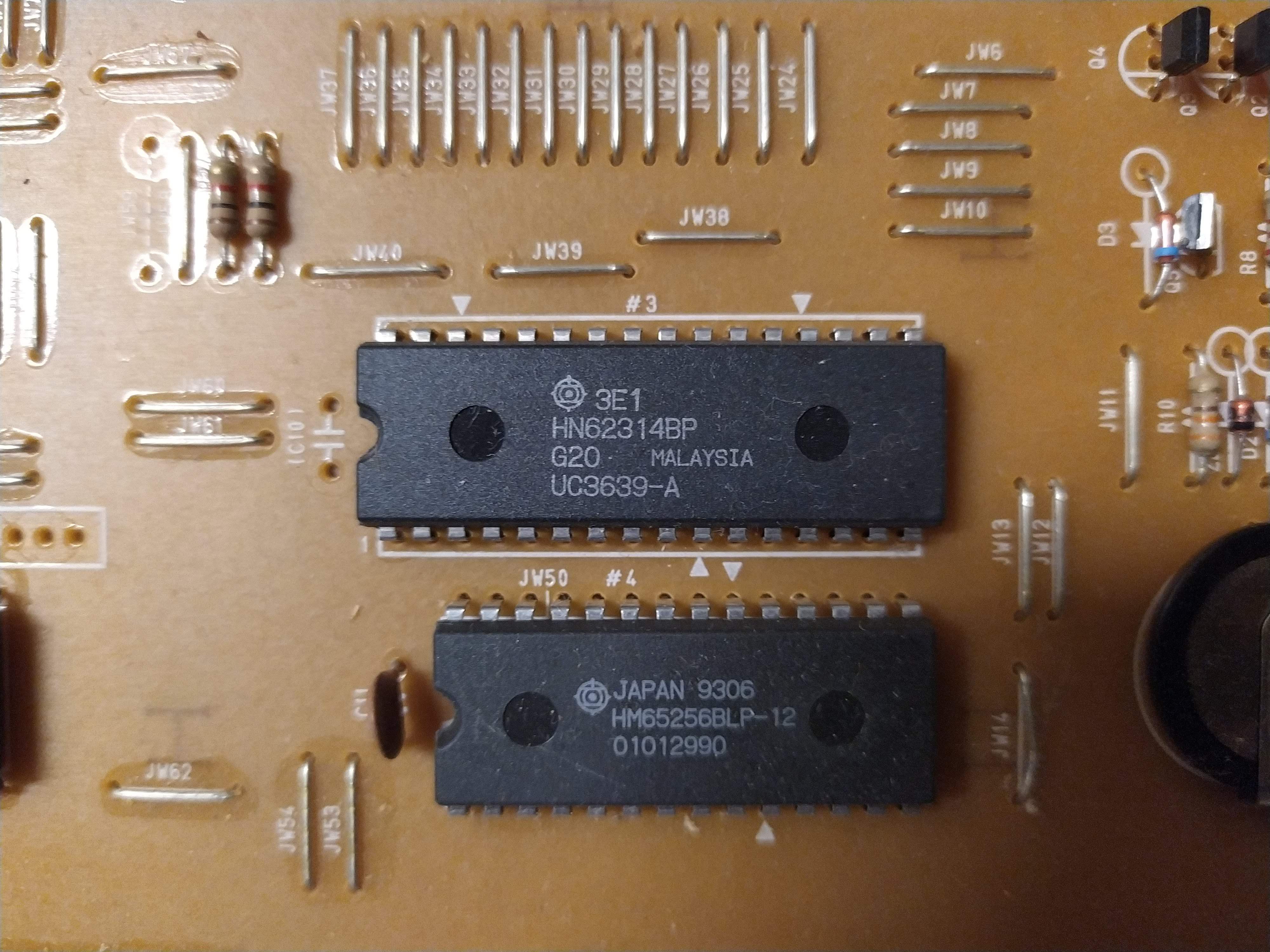
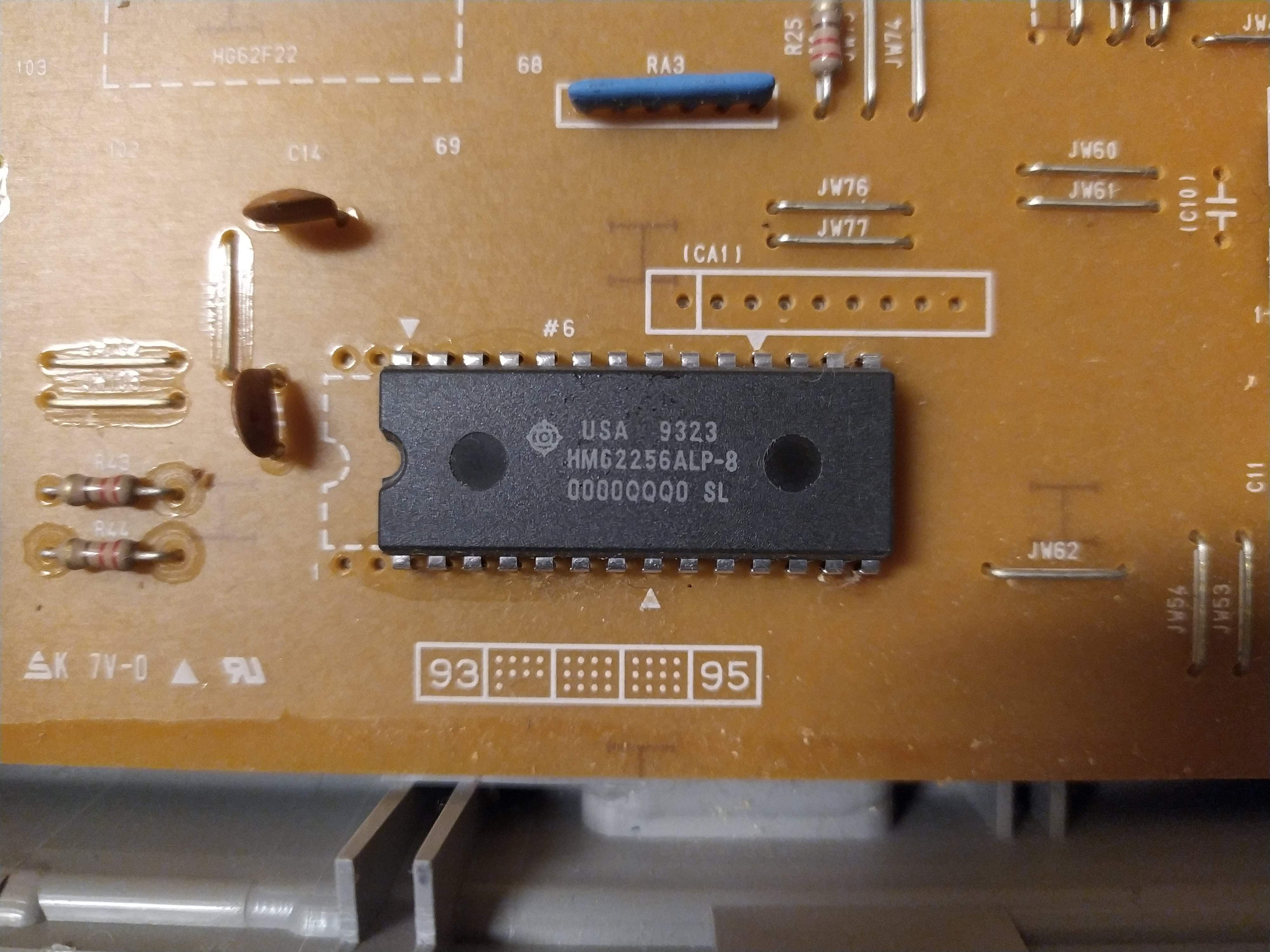
Hacking the Brother WP-1250
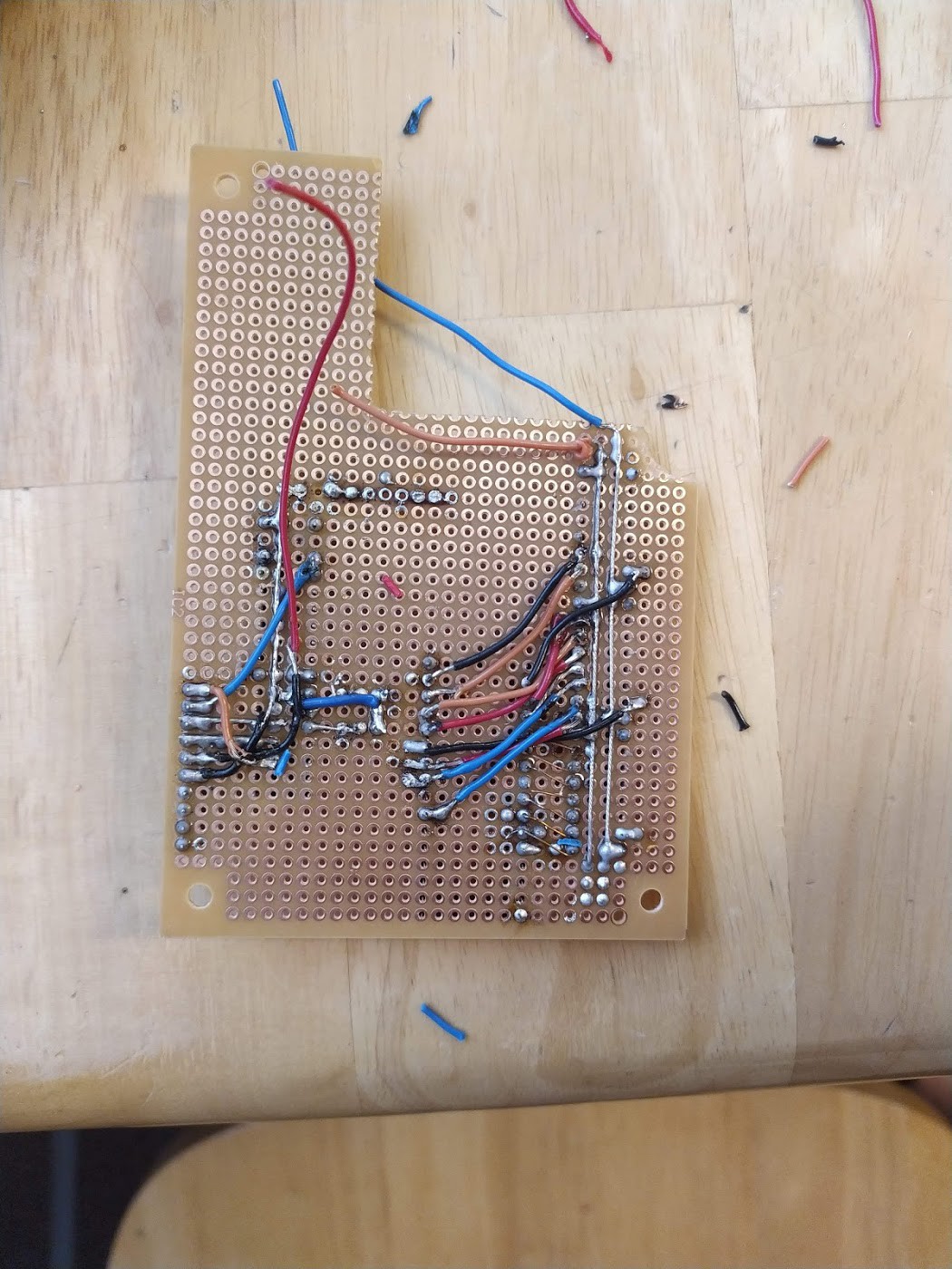
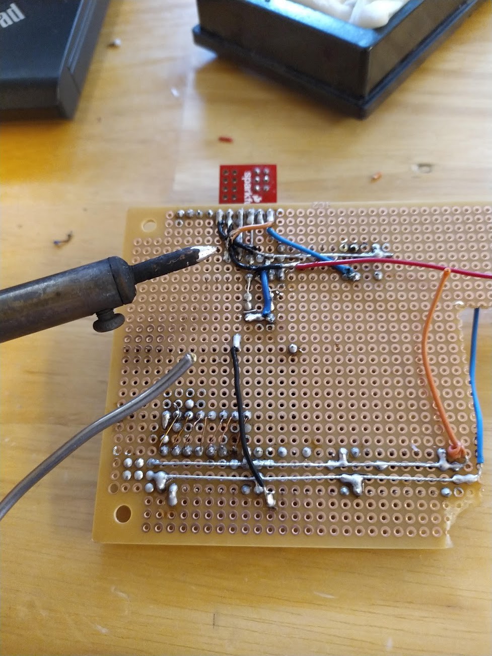
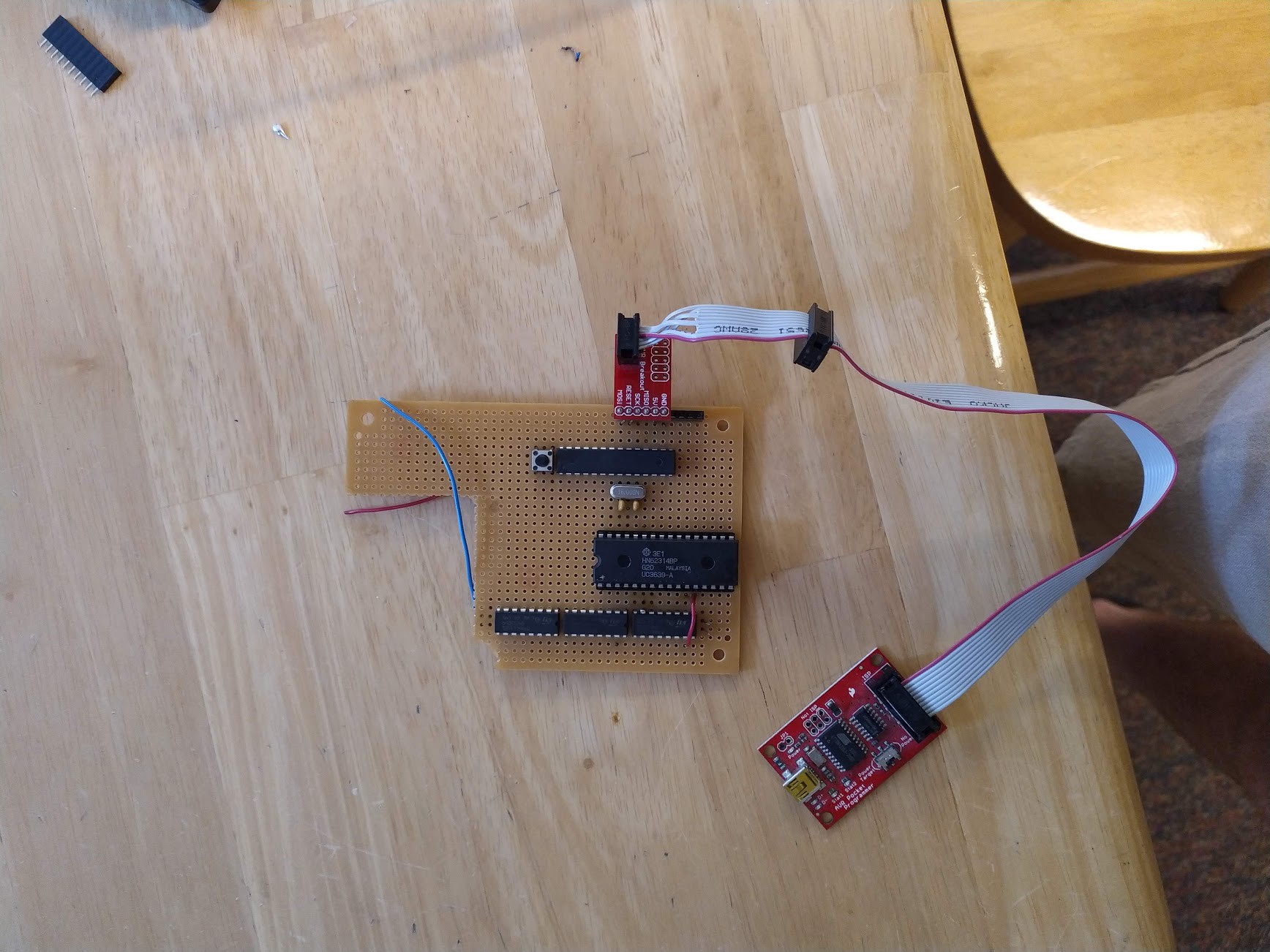
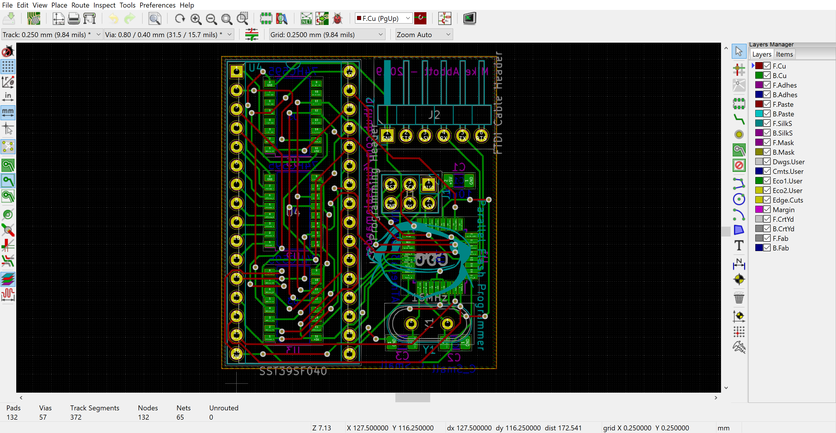
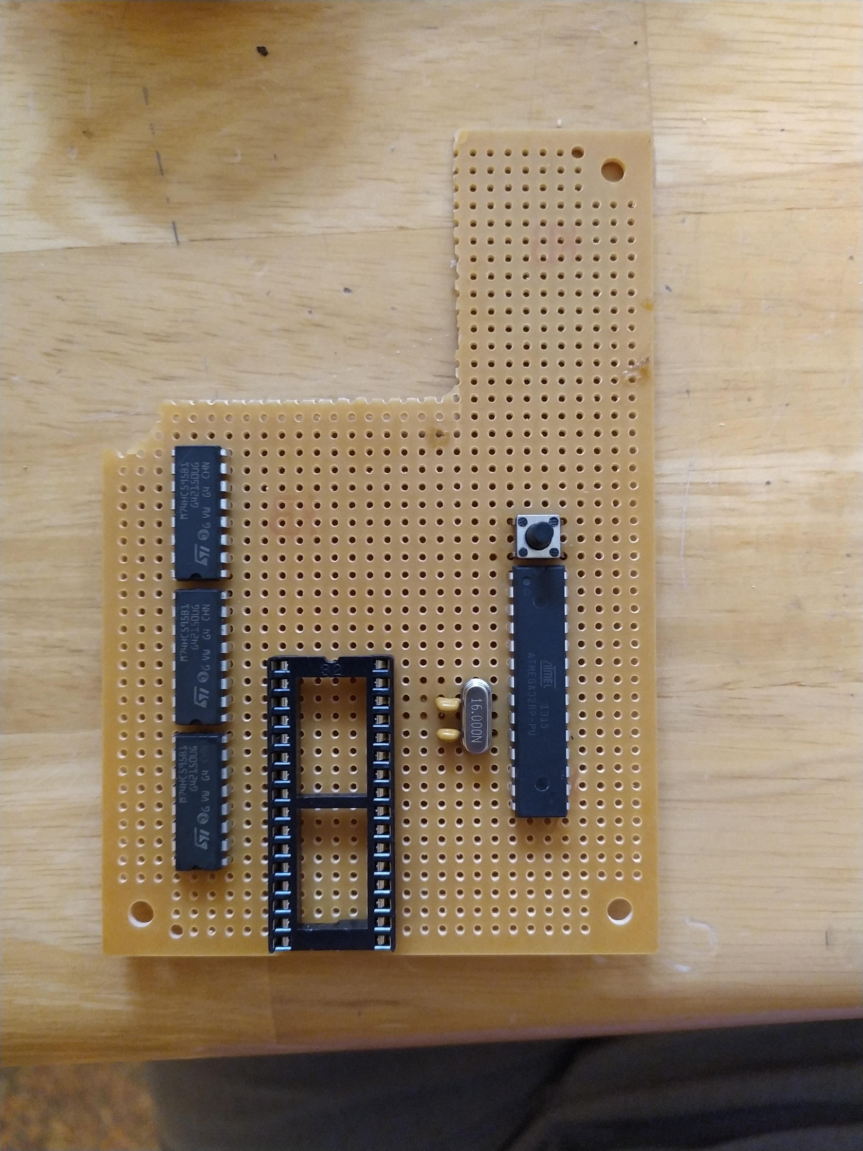
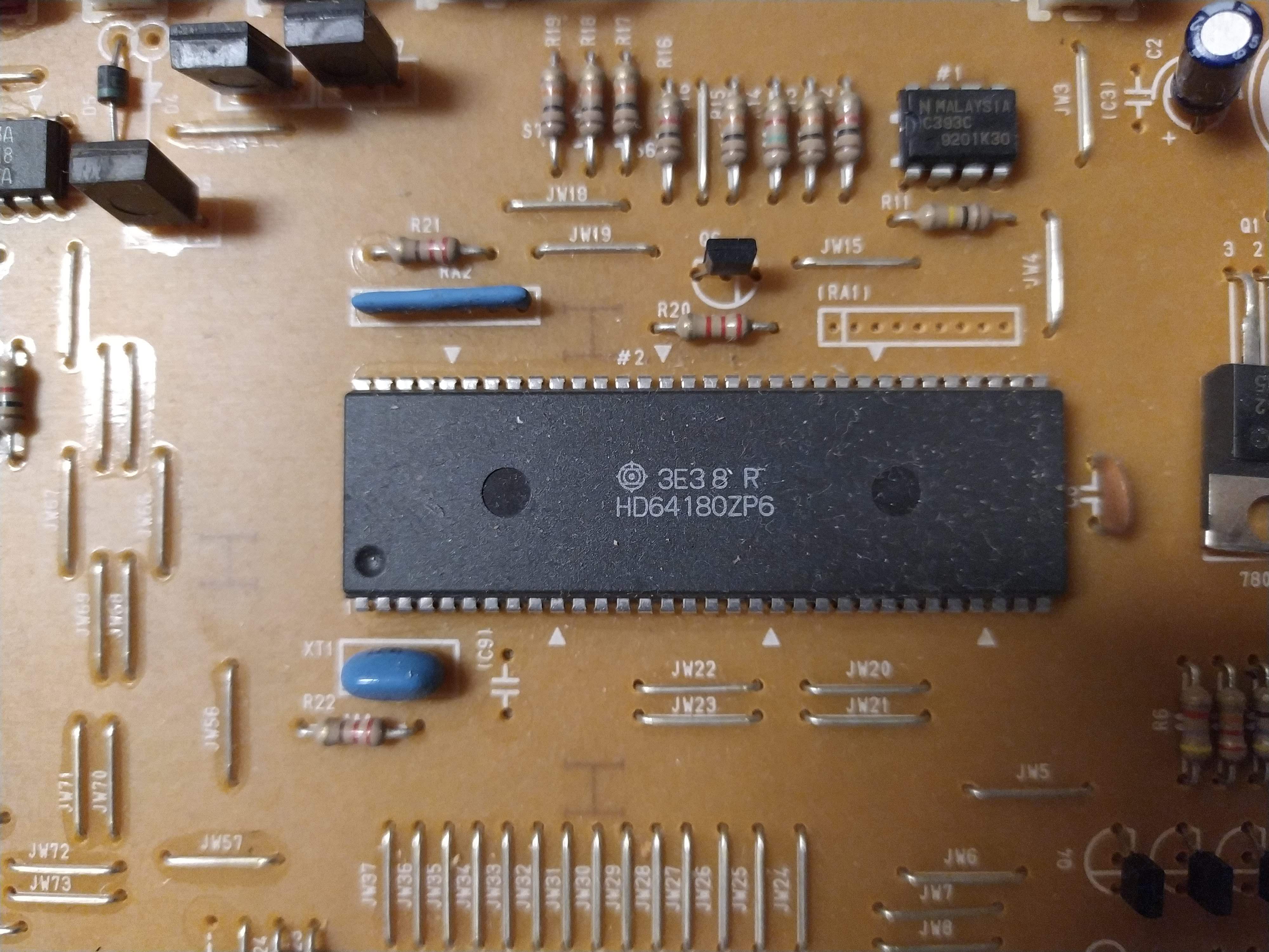
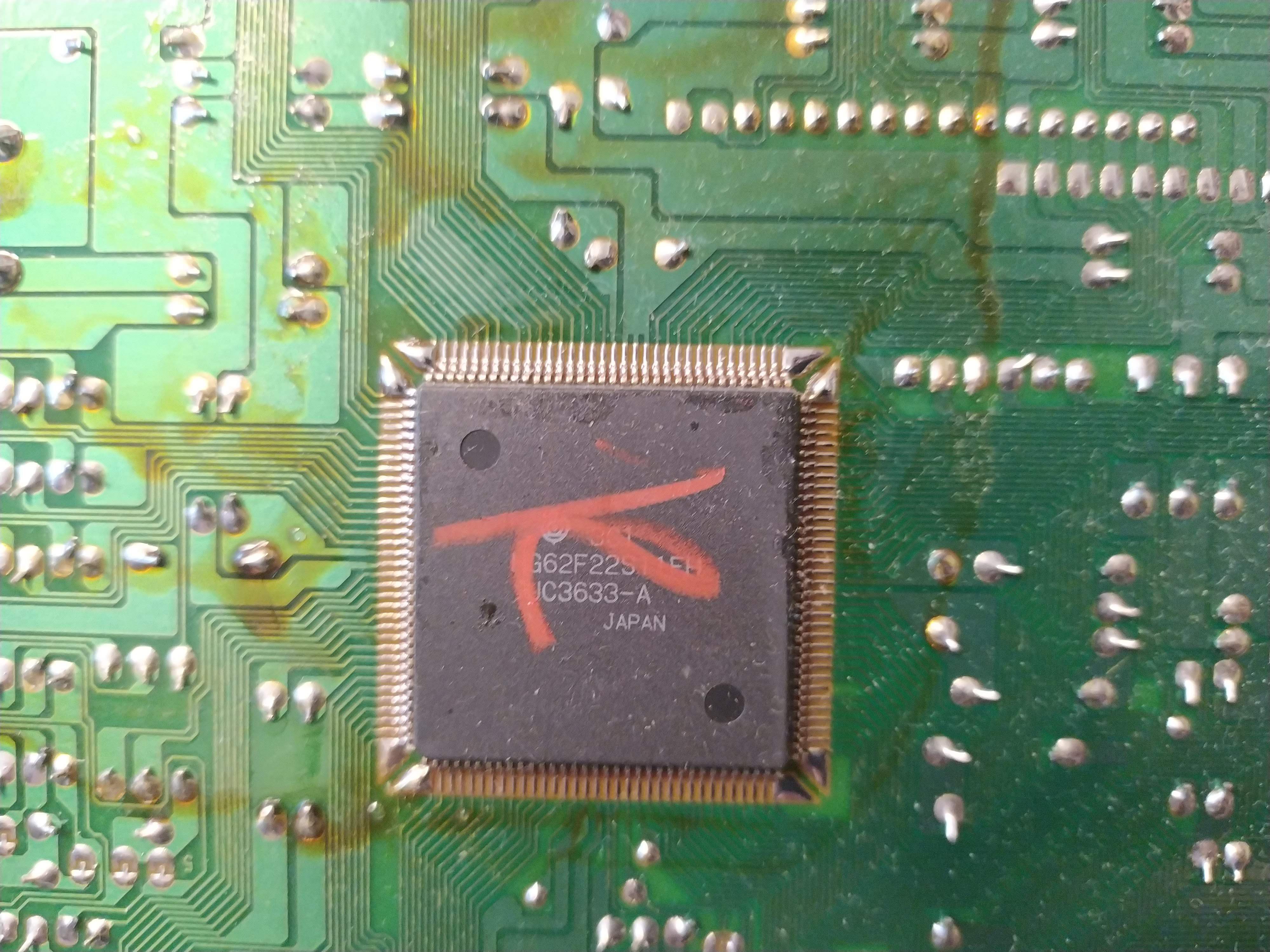
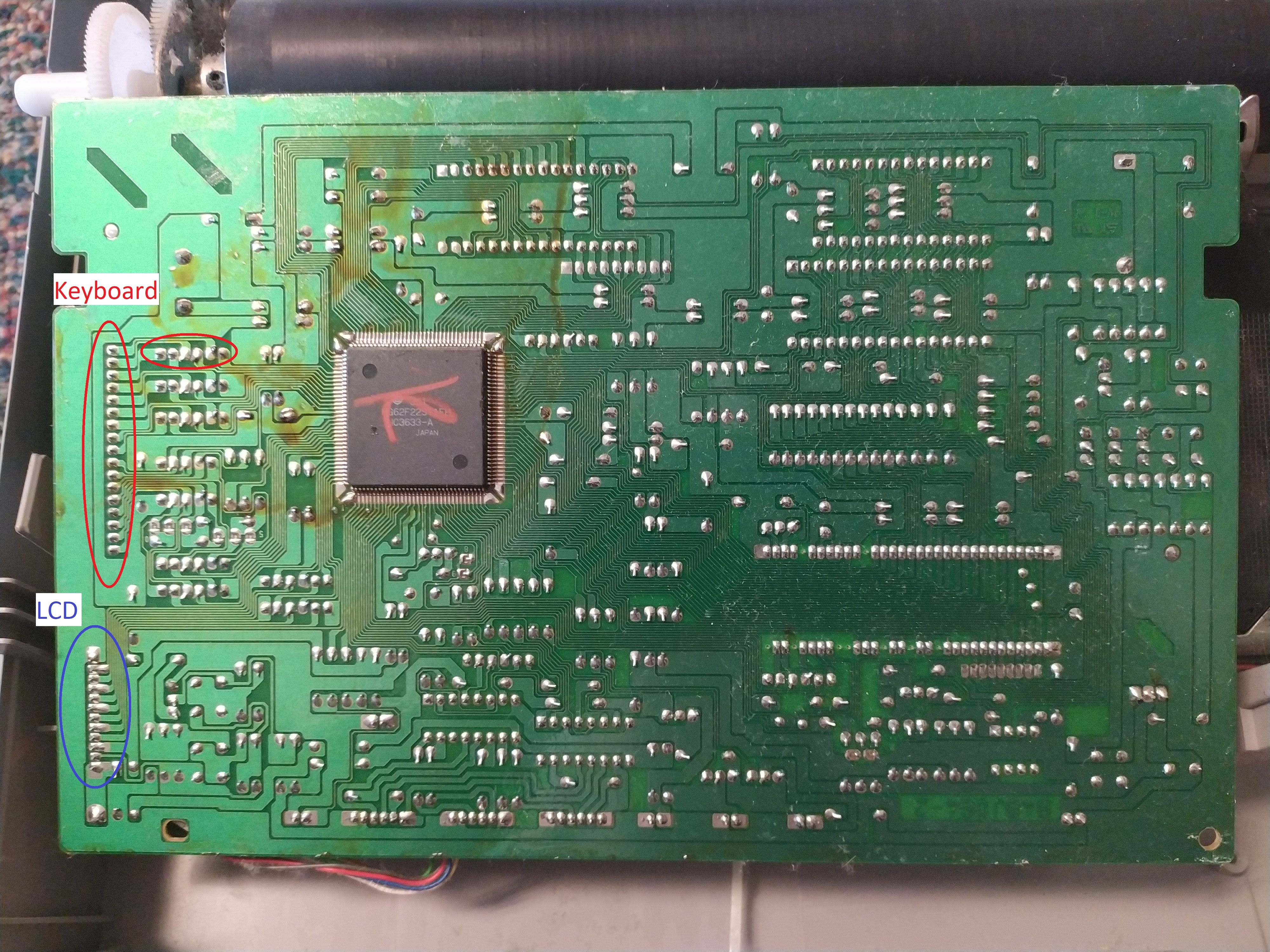
Modifying a word processor/electronic typewriter from the 90s. Long term goal is to get this thing to load retro.hackaday.com
 furrysalamander
Become a Hackaday.io member
Already have an account? Log in.
Just one more thing
To make the experience fit your profile, pick a username and tell us what interests you.
Pick an awesome username
hackaday.io/
Your profile's URL: hackaday.io/username. Max 25 alphanumeric characters.
Pick a few interests
Projects that share your interests
People that share your interests
 Anders Nielsen
 Alex Brown
 Dave Collins
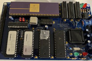
 Ross Bamford