 Max.K
Max.KTwo days ago the PCBs from OSH Park arrived. The quality is incredible considering that I paid just over 5€ for three boards:
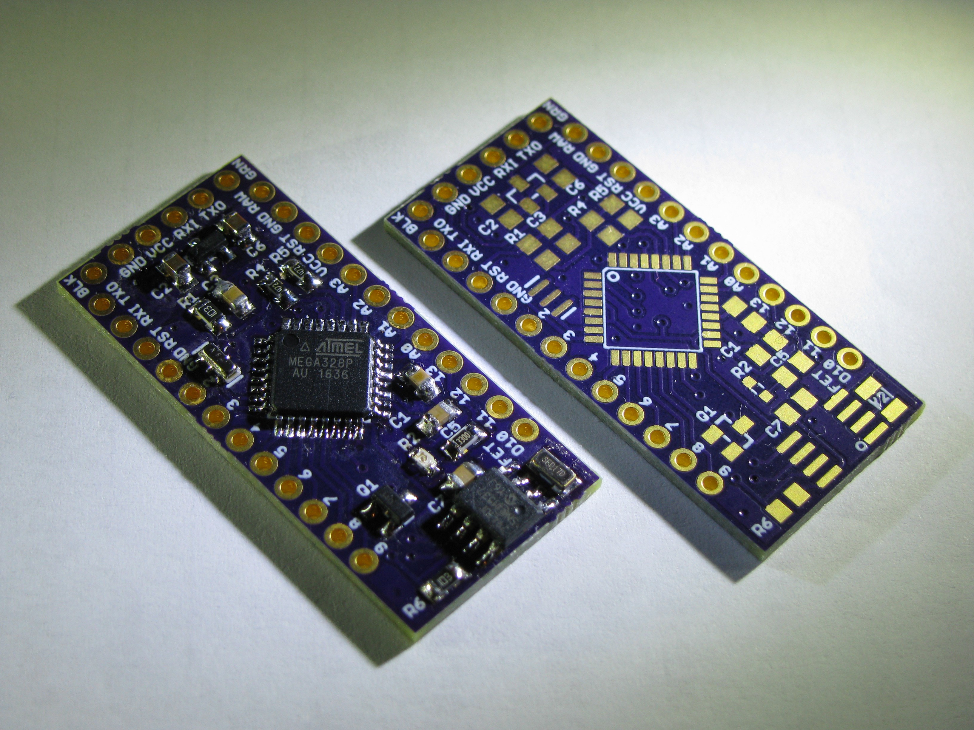
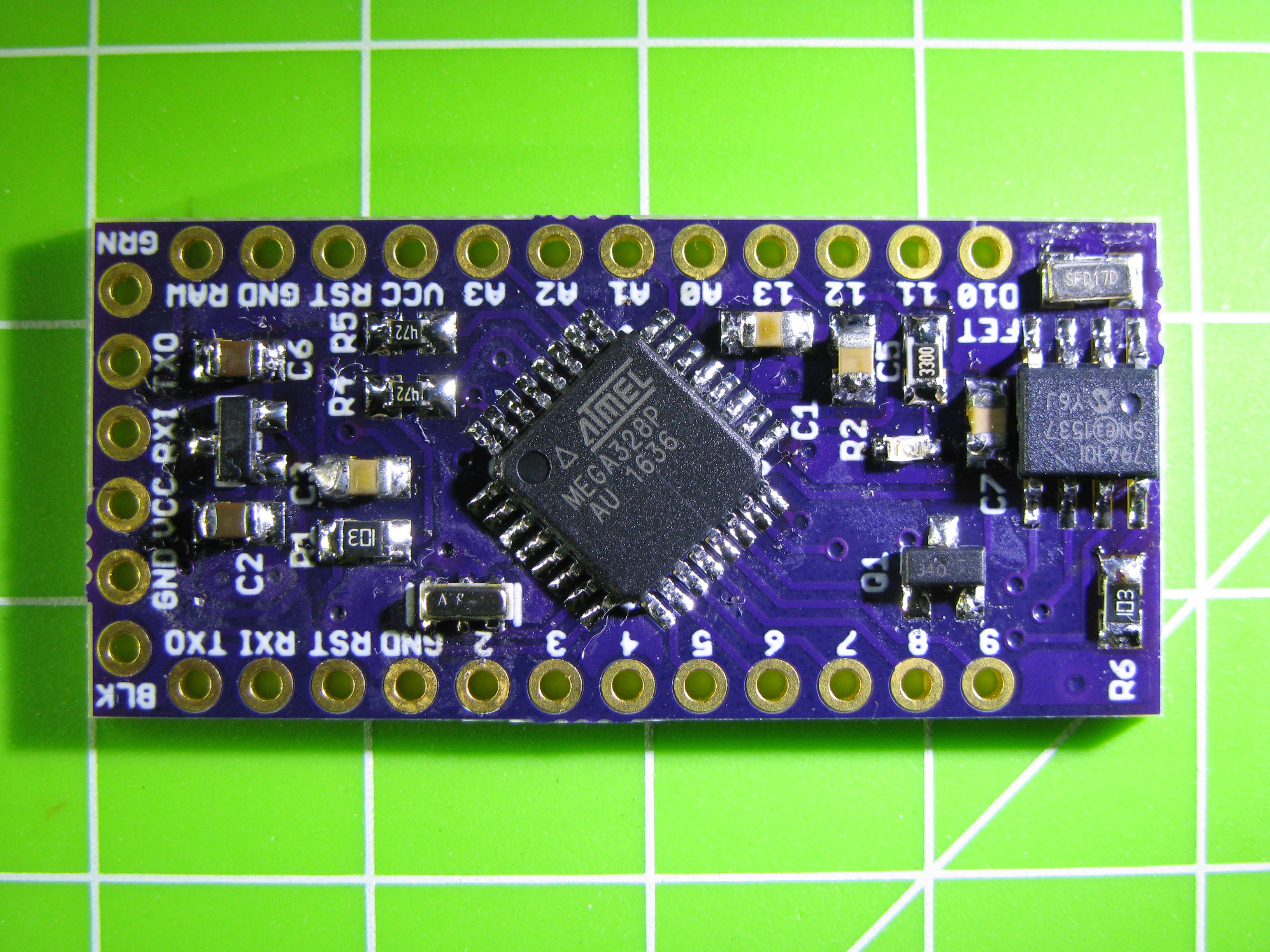
After soldering the few components onto the board and flashing the bootloader, everything seems to be working perfectly.
The new voltage regulator is supplying 3 V as expected. The real time clock is running and can already generate a 1 Hz signal for testing the interrupt. This can be used to wake the ATmega from sleep. Even the Mosfet works, which can turn off high power components.
Now for the interesting part: Power consumption.
With the ATmega running, the board draws about 6.3 mA at 5 V (supplied by an Arduino Uno). This is nothing exceptional. But after the alarm is set and the ATmega goes into sleep mode, the current consumption goes down to only 2.8 µA. At this point only the RTC is active with a timekeeping current of 1.2 µA (according to the datasheet). Also the regulator is wasting around 1 µA.
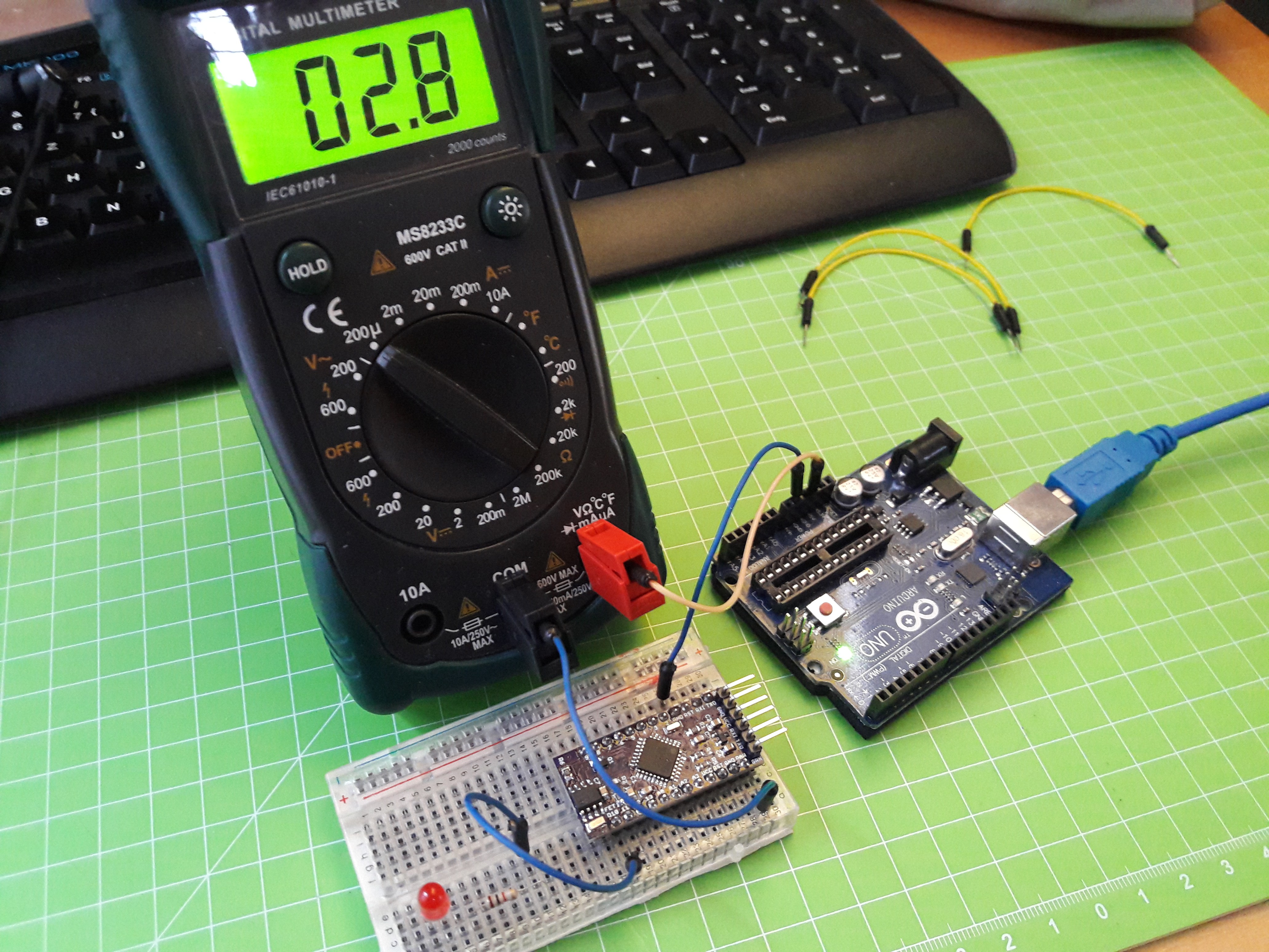
I am not sure it the sleep current could be reduced even further but 2.8 µA is already extremely low. As an example, if the board has to wake up every 5 minutes for one second, it will run for almost a year using only a 240 mAh coin cell. With AA batteries it would be around 10 years.
In terms of software, I already implemented some basic functions for settings an alarm. The goal is to have a RTC-delay function that wakes the ATmega from sleep after a certain amount of time.
Discussions
Become a Hackaday.io Member
Create an account to leave a comment. Already have an account? Log In.
Hmm... where are the A4 and A5 pins? How am I supposed to connect my I2C sensors to it?
Are you sure? yes | no
Oh, I didn't notice that until now. While designing the PCB there was not much room left for pins, so I thought more than 4 analog pins would not be necessary. Somehow I didn't realize that I need those for I2C. Not very smart... :(
That means I will have to make a second version. As a temporary fix you could of course solder wires to the real time clock or use software I2C.
Thanks for finding that error!
Are you sure? yes | no
but don't you have R4 and R5 as pullups on those pins? makes it somewhat connectable, soldering I2C to the resistors.
Are you sure? yes | no
Yes, R4 and R5 are connected to SCL and SDA. The RTC is also connected via I2C, so you could use its pins as well. Dedicated A4/A4 pins should be included though, I really forgot about those.
Are you sure? yes | no
I think it's a good idea to break out all pins (including the analog-only A6 and A7, and maybe even the two XTAL ones), even if only as pads at the bottom (a la teensy). The reason is, you are obviously targeting more advanced users, and they will always want to do more...
Personally, I could never understand why the Pro Mini has the GND, RST, VCC, TX and RX pins duplicated (GND is there 3 times, actually), but then has the A4, A5, A6 and A7 in such weird places, and no XTAL pins at all.
Are you sure? yes | no
Those are good suggestions. I will try to put A6 and A7 on the bottom as pads. The Mini really has a strange layout. I just wanted to base my design on an existing board rather than making another entirely new board.
Are you sure? yes | no