 Patrick Van Oosterwijck
The design as implemented from the original idea has the following features:
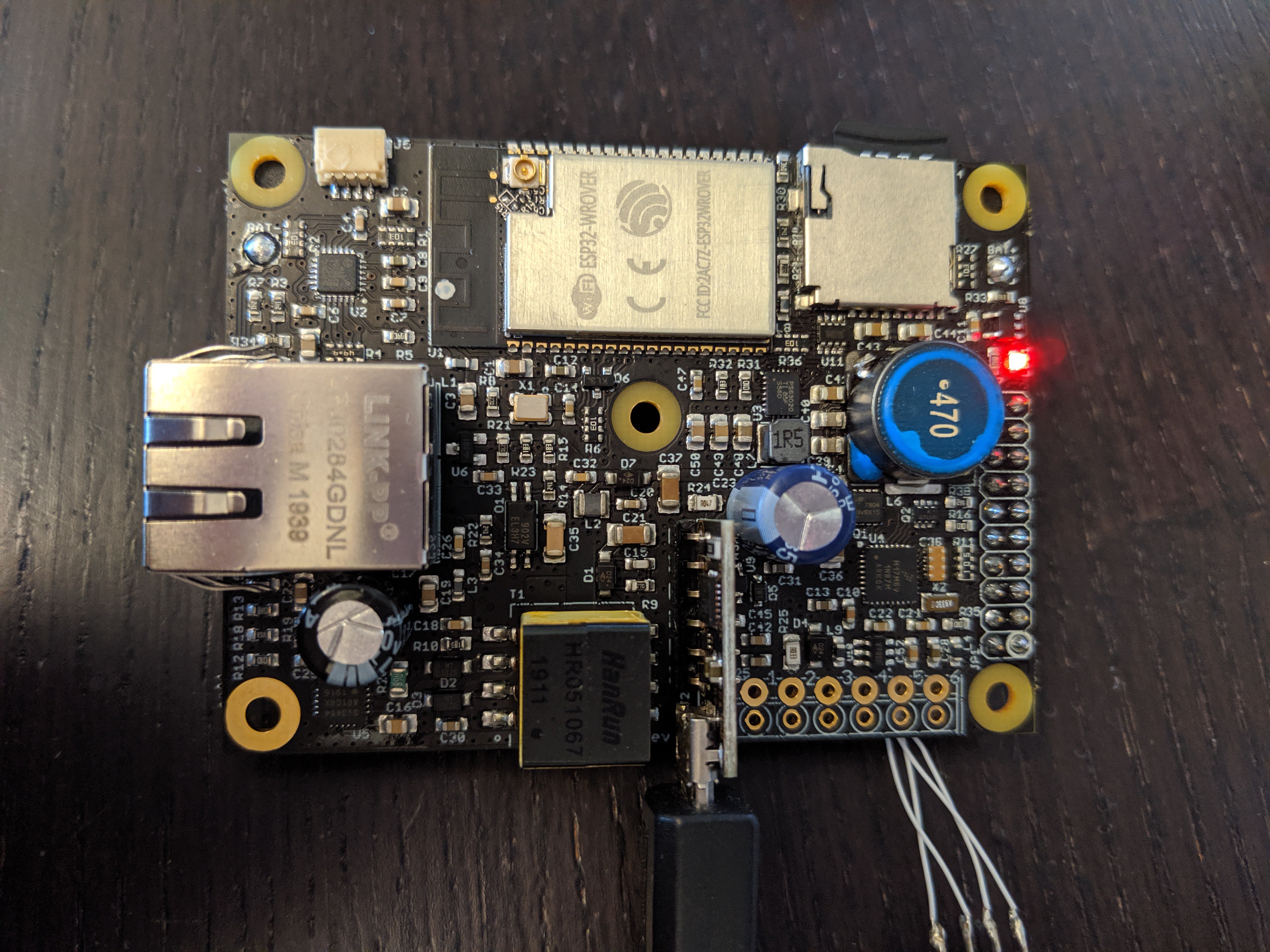
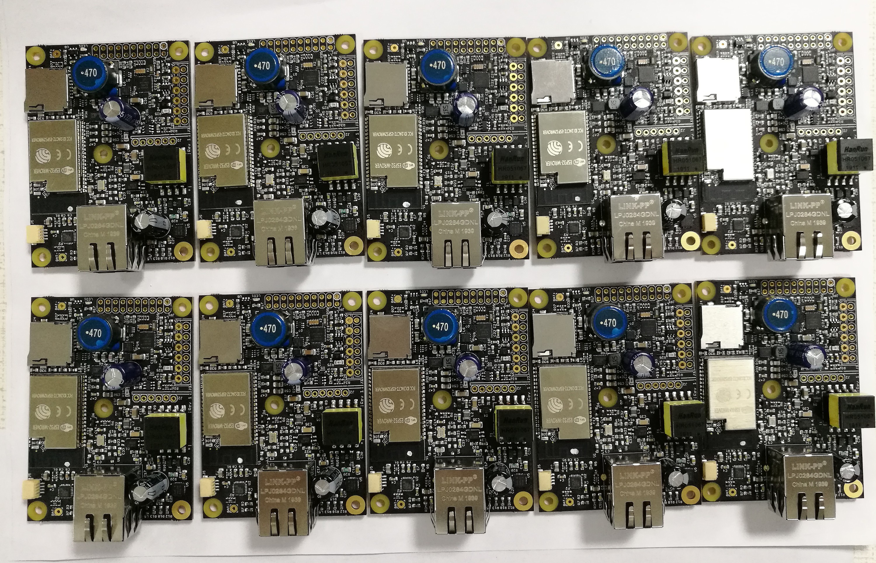
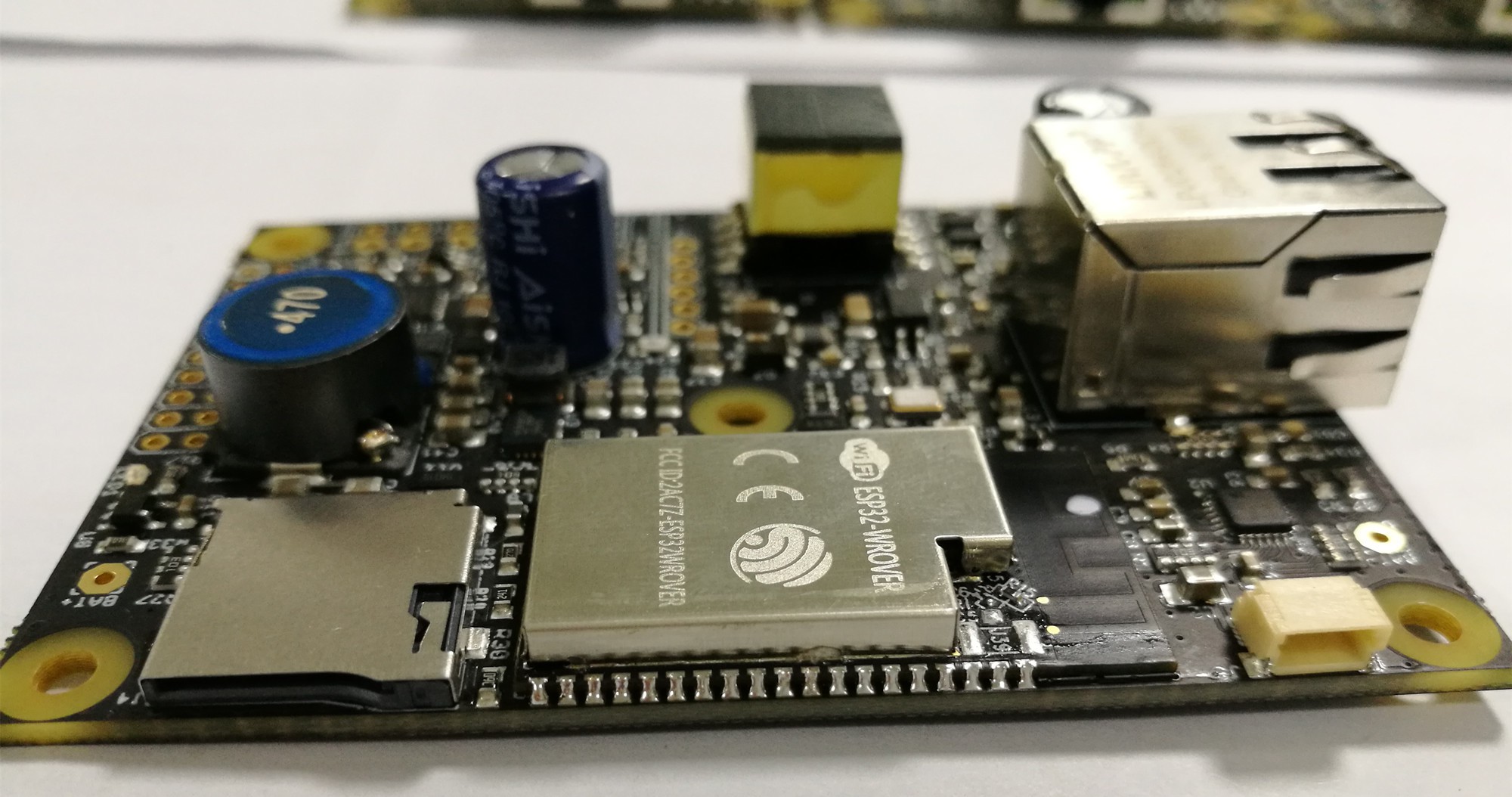
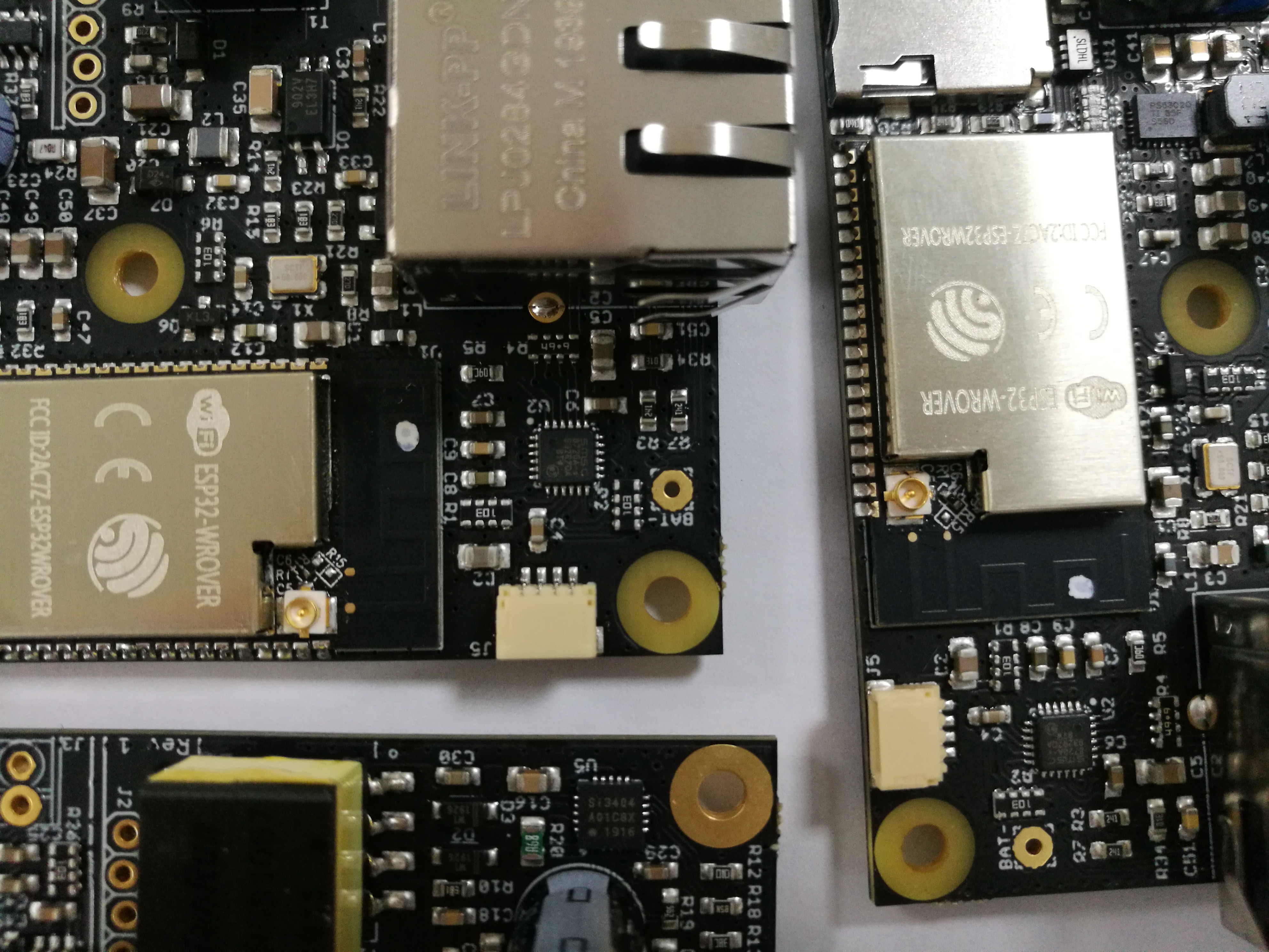
Processing system
- ESP32-WROVER-I module with 4 MB Flash, 8MB PSRAM and external U.FL antenna connection
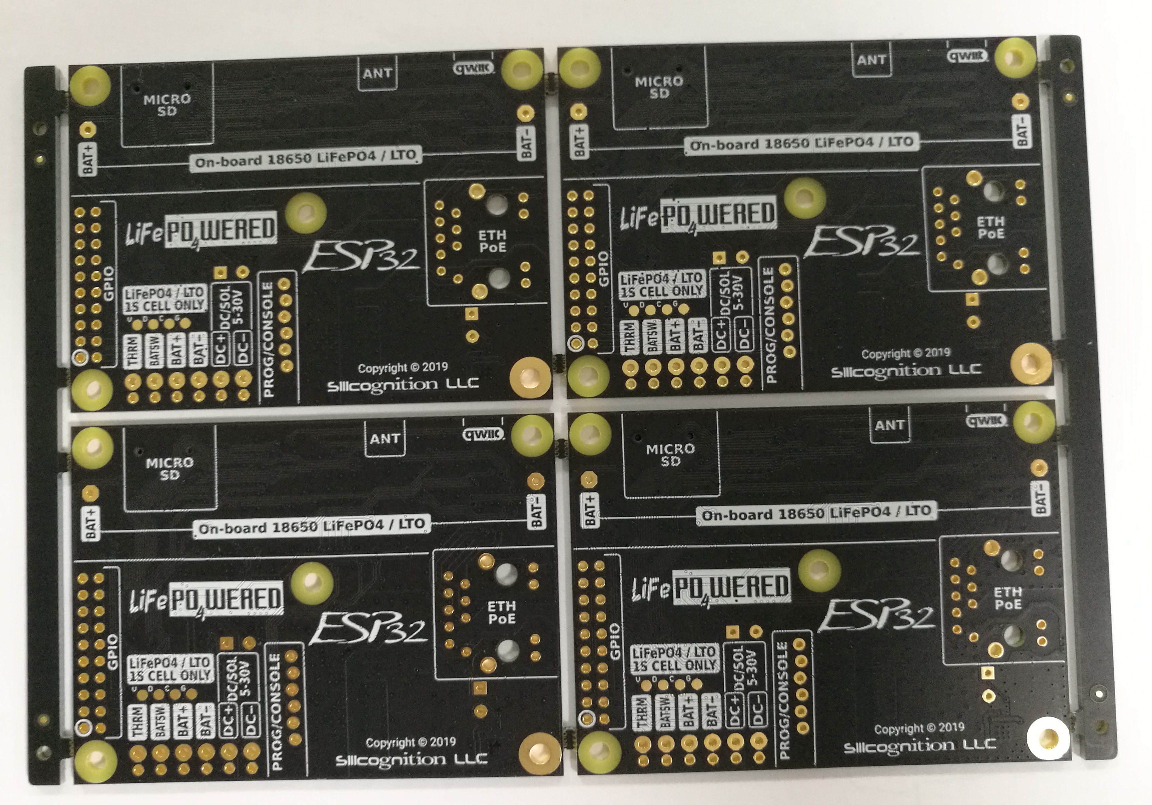
- Micro SD card slot for data storage
- Separate NXP MKL17Z32VFM4 ARM Cortex-M0+ charge / system controller allowing ultra low power sleep with various wake events including RTC
- Charge / system controller fully configurable by ESP32 over I²C bus
Power
- Battery-backed: either by LiFePO4 cell or Lithium Titanate (LTO) cell for highest reliability due to predictable power on/off behavior and buffering of erratic input power
- Long life with typically 2000+ cycles at 100% DoD when used with LiFePO4 cell
- Extremely long life with typically 10000+ cycles at 100% DoD when used with LTO cell
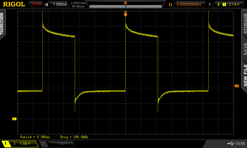
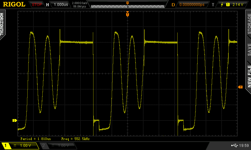
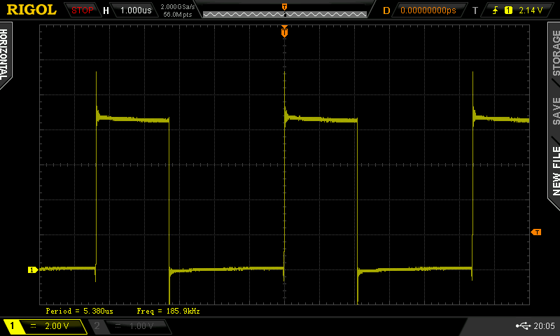
- MPPT charger to efficiently extract the most energy from a connected external power source
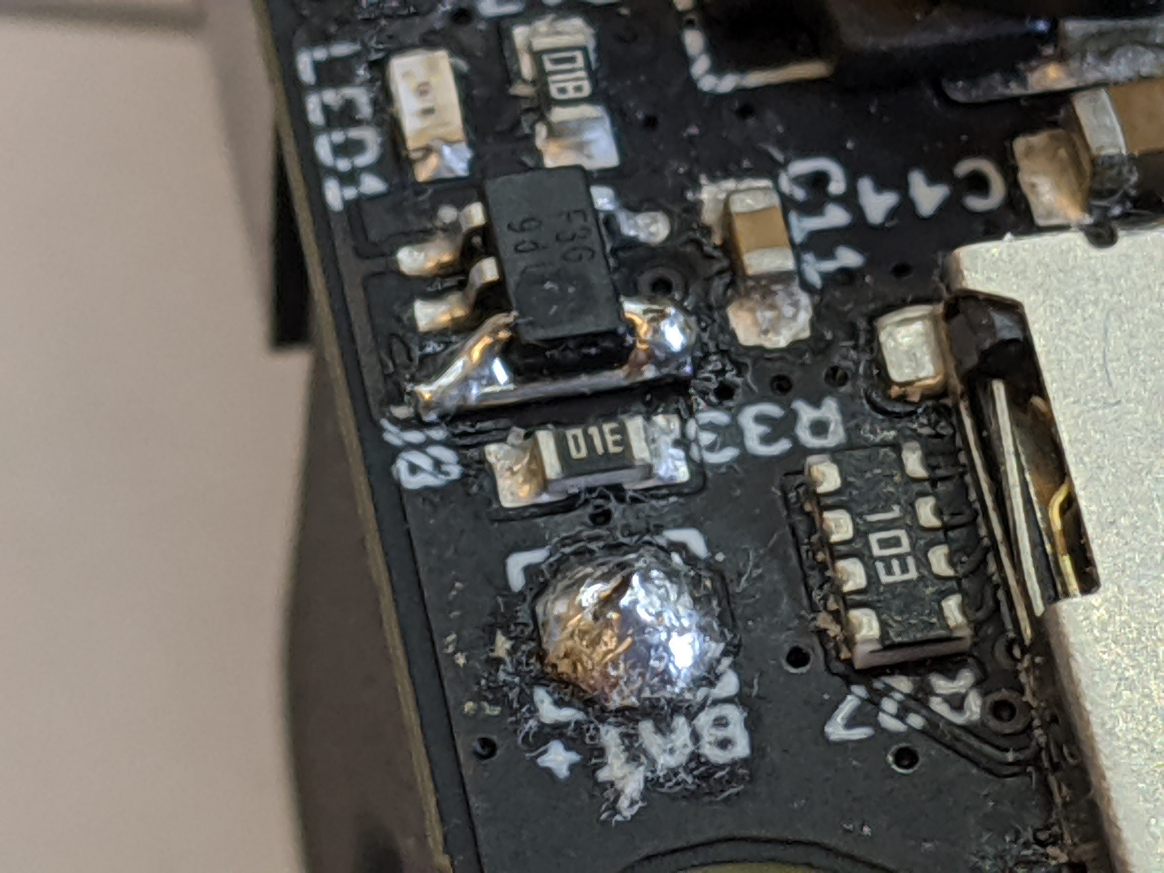
- Convenient battery and external power connection with screw terminal block
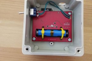
- On-board 18650 battery option
- External power option DC 5V - 30V
- External power option solar panel 5V - 30V
- External power option micro USB 5V through optional wESP32-Prog module
- External power option isolated Power over Ethernet IEEE 802.3af
- OR'ed external power inputs can be present simultaneously
- Integrated buck-boost to provide regulated 3.3V to the ESP32 system
Connectivity
- WiFi 802.11 b/g/n using external antenna connected to the U.FL
- Bluetooth 4.2 with Low Energy (BLE)
- 10/100 Mbit Ethernet
- GPIO header with UART, I²C, SPI, etc.
- Sparkfun Qwiic connector allows easy solder-free development using existing Qwiic modules
Physical
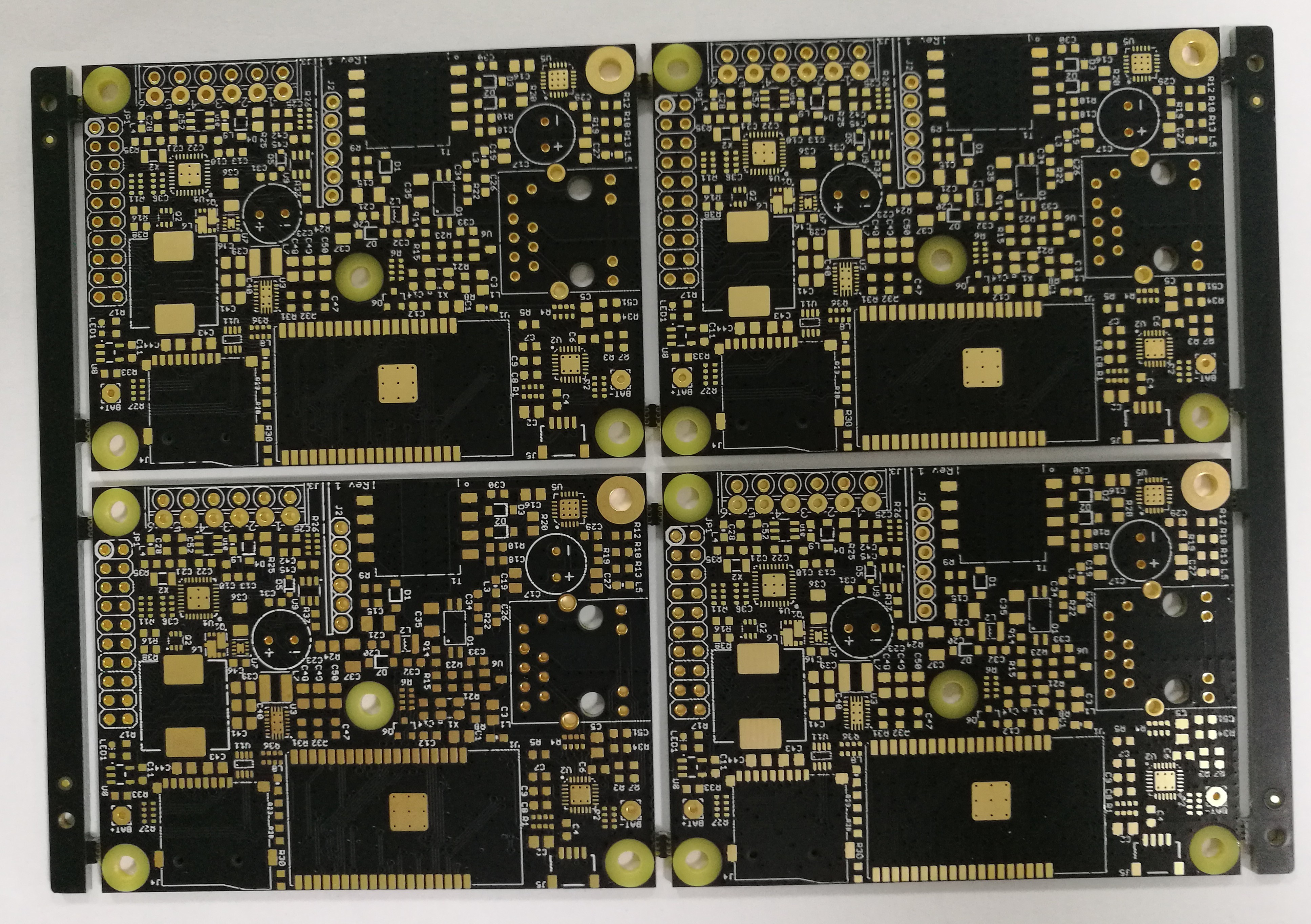
- Compact 75 mm x 55 mm PCB
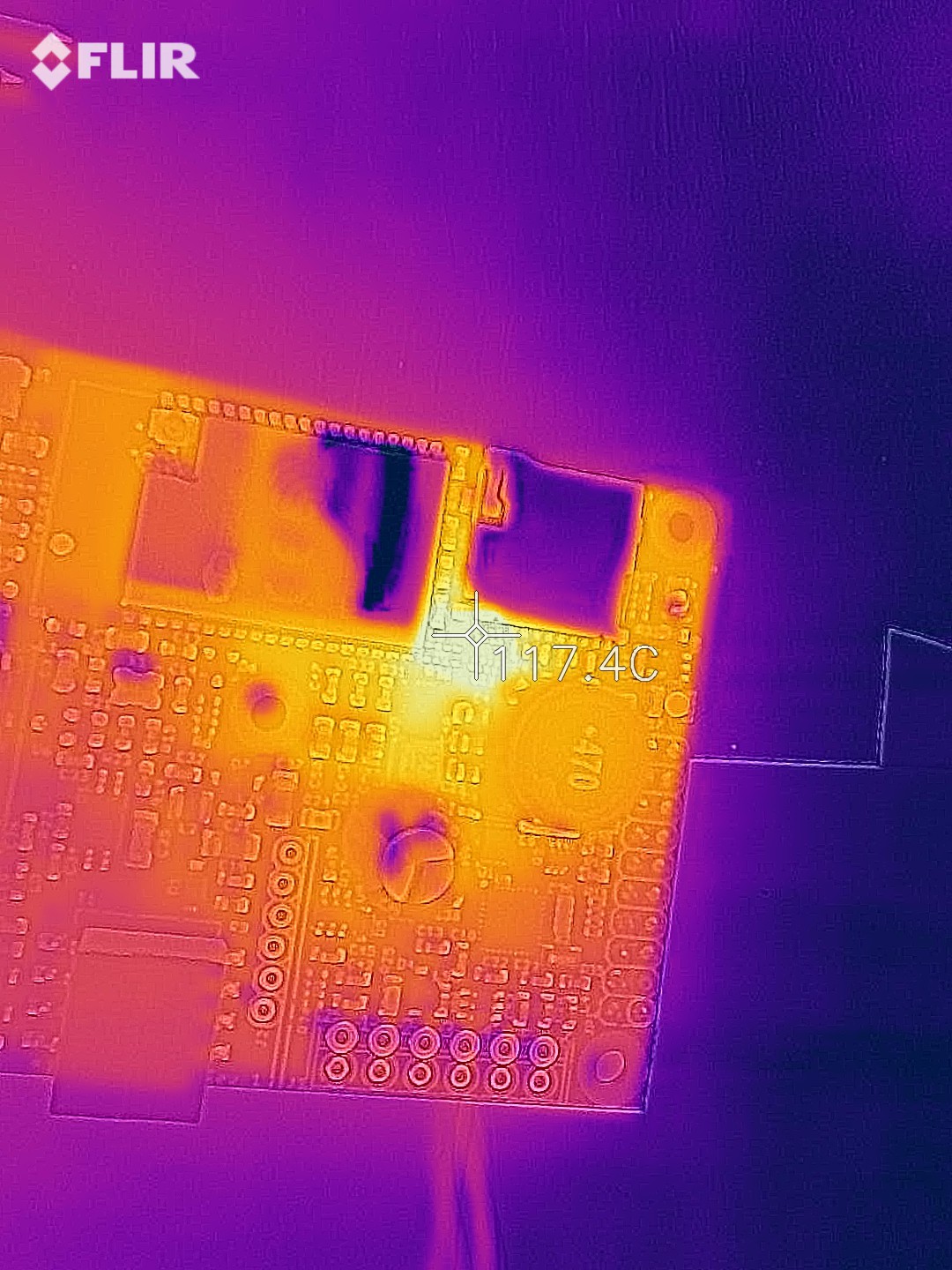
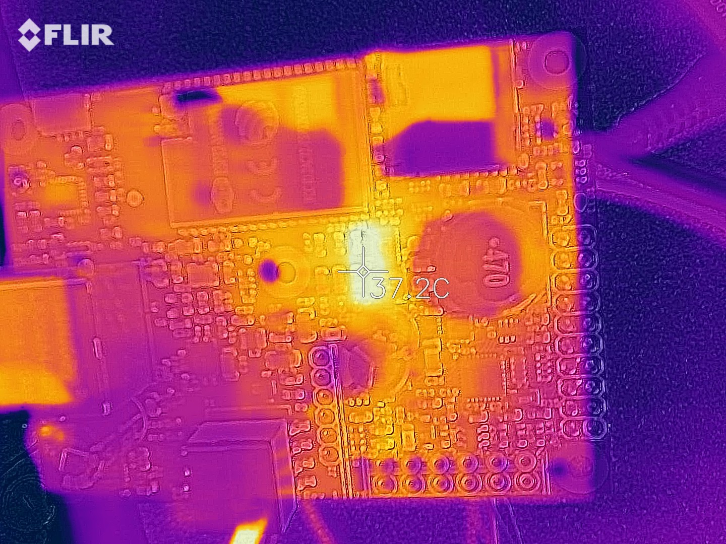
- Designed for wide -40°C ~ 85°C temperature range
- Battery heater option for charging LiFePO4 in cold temperatures (not needed for LTO)


 David Scholten
 Dan Julio
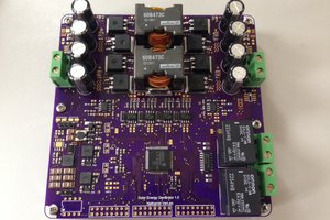
 Nathaniel VerLee
This is an exciting project, I ESPecially like the use of LTO batteries to complement a Solar panel. Excellent! Were you able to get this board working? I'm trying to do something similar, minus the PoE, which I now want having seen yours!