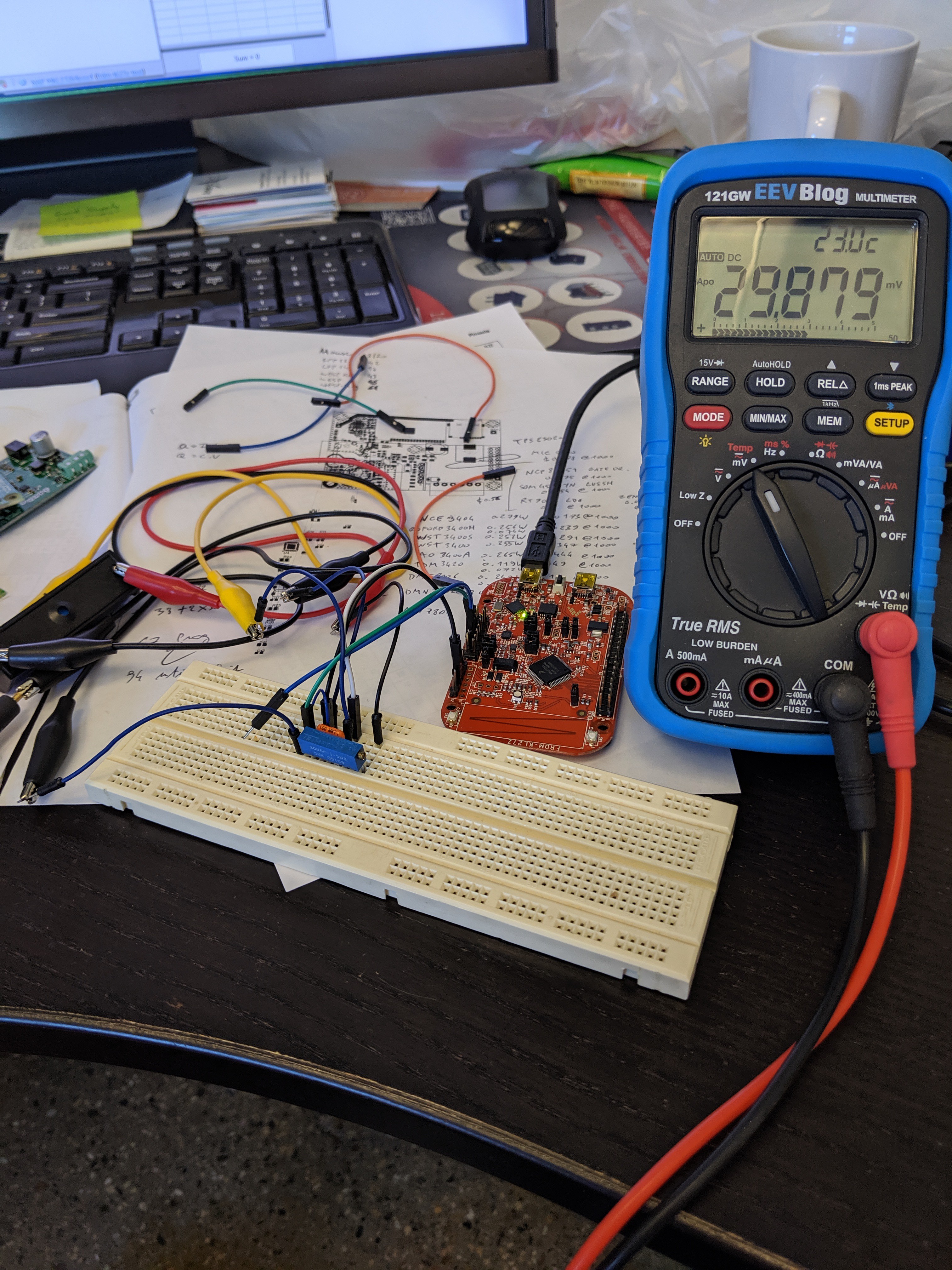
I got a FRDM-KL27Z development board to be able to test some things in the design before committing to them in a PCB layout. Initially I had intended to use this to build and verify the complete charge buck converter, but that was before I realized I need a proper gate driver. I am no @greg davill, you won't see me put together a dead bug prototype with 0.5 mm pitch QFNs under a microscope. So a complete charge converter prototype won't happen before the PCBs are made.
But, I decided the dev board would still be useful to do some testing of the ADC for current sensing. One of the reasons I chose the MKL17Z64VFM4 is because when I was designing the custom project this is based on, I liked the built-in ADC and reference of the MK02FN64VLF10 I was using for that project and found I could do current sensing directly with the micro using the differential 16-bit ADC inputs. I decided I should verify whether this chip worked as well for the purpose.
Battery heater decisions
Surprisingly, the need for ADC data came out of the need to settle on a particular implementation for the battery heater driver. I am driving the heater from the battery voltage in this design. The idea is to again make things more automatic and easier for the user. In the #LiFePO4wered/Solar1, I drive the heater from the incoming voltage. The downside is that no MPPT happens, the heater has to be carefully designed to not overload the solar panel and make the voltage collapse. In this board I want to power the heater from the battery (much more predictable), and supplement as much power from the external input as available. I also want to use the solar power most efficiently, so MPPT is desirable for the heater power. Instead of building a completely separate MPPT converter for this purpose, I'm using the charger MPPT converter and divert all available power to the heater up to the point where all power comes from the input.
There are two topologies I considered:
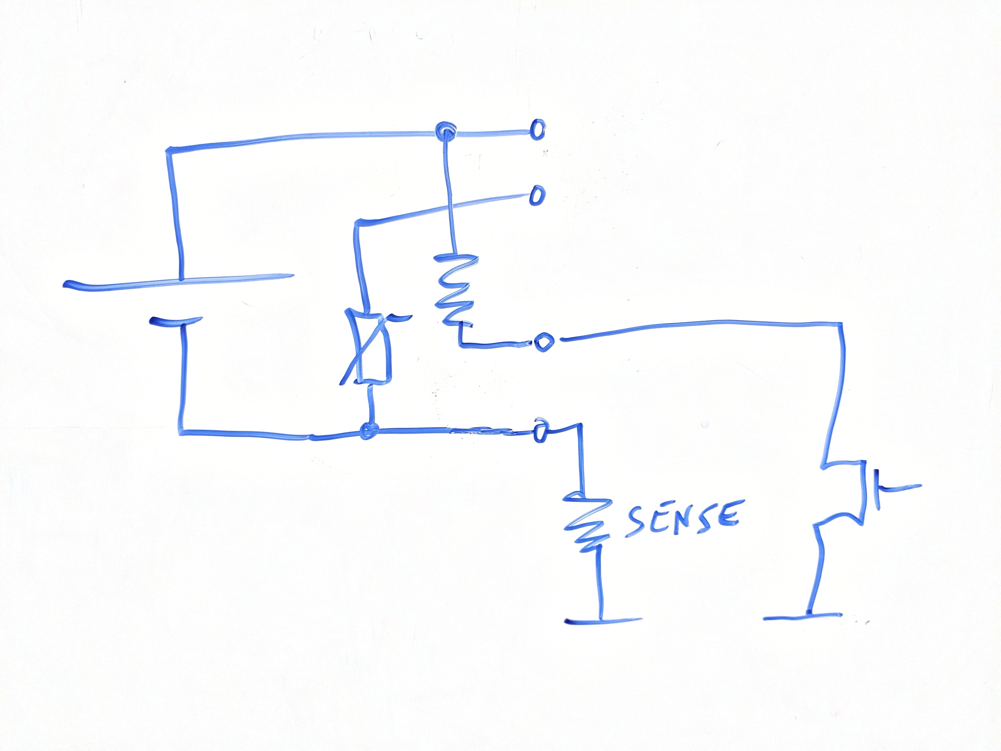
Heater connected to battery ground, driven by an external voltage. This requires the board to drive a voltage to the heater. Just using a MOSFET to switch this voltage isn't safe, the output needs to be properly protected so I would preferable be using a load switch.
The other option is to connect the heater to the battery's positive terminal, and pull the other end to ground from the circuit. I looked hard to find low side load switches with integrated current limiting, but for the life of me I couldn't find anything suitable. If anyone has suggestions I'm all ears. So this would most likely be implemented as a MOSFET with thermal fuse. I'm not a fan of thermal fuses, they are kind of sloppy.
In topology 2, you can see a single current sense resistor. It's the battery current sense, but it can also measure the heater current. More correctly: it can measure whether the heater driver is diverting all power from charging the battery to heating the battery. We may not know what the current is exactly, but we know when the battery current is zero and can implement something in the MPPT control loop to maintain this.
In topology 1, you can see two current sense resistors. One is to measure the battery current, the other measures the heater current. It is necessary to add the second current sense resistor because the battery current sense provides no visibility into the heater current, we sense the current whether it flows through the battery or the heater. The upside is that we still know the absolute current value. We can build a control loop to make the heater current match the battery current. The downside is that we need another current measurement, and it is a high side current measurement (near supply voltage). This means we have to use a differential ADC channel for this.
Testing the ADC
"Remember kids, the only difference between screwing around and science is writing it down." — Adam Savage
Current sensing near either ground or supply is always potentially problematic. The datasheet of the micro doesn't specify the common mode range of the differential ADC channels. It depends on the actual circuitry implemented in the chip how well measuring near ground and supply works. That's why it needs to be tested. The voltage across the battery current sense resistor can actually be positive (charging) or negative (discharging) with reference to ground. Of course, it's a tiny voltage of only 30 mV or so, but still, not all input stages can handle signals near ground, near supply or both.
I started screwing around with the dev board two days ago, but I saw some interesting/weird things that made me decide I needed to actually collect data and write it down (science!). That's what I did yesterday.
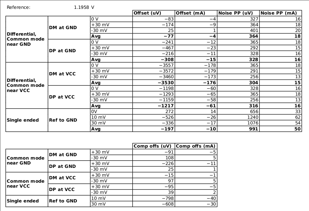
Here are the results:
In the top table I measured differential input near ground and supply, with either input pin tied to the power rail, and with zero, positive and negative input relative to the power rail. I also tested a single ended channel (referenced to chip ground) for comparison. Because I have only two differential inputs, if I choose topology 1, I will need to use a single ended input for the current coming in to the charge converter, so I need to know how well it works.
The offset indicates the difference between what the micro measured and measurements taken with my 121GW meter. Noise PP is the worst peak-to-peak noise on the raw measurements over 100+ readings.
Currents in the table are based on a 20 milliohm current sense resistor. This value is a compromise to get usable readings for 1.5 A charge current range while not burning too much power, and is still subject to change. Higher values give better readings but reduce efficiency, so a good balance has to be found. 20 milliohm is just a starting point to be able to reference the numbers to real life application data.
In the second table, I check how well the data can be offset compensated by taking a baseline at 0 V (zero current through current sense) and using that to compensate the raw readings.
Some thoughts on the data:
The offset seems to be different depending on whether DM or DP input is connected to the supply rail. I don't know how to explain it. I had maybe expected a difference depending on whether the reading was inside or outside the supply range, but that doesn't seem to be the case. A difference between the two differential inputs is unexpected.
Offset is much worse near supply compared to near ground. Especially with DM at supply, the offset is bad.
That said, it seems the offset of the differential channels is consistent and can be compensated for quite well by establishing a zero current baseline. This seems to be the case both near ground and near supply. 5 mA offset is perfectly fine for a 1.5 A range (0.3%).
Performance of the single ended measurements is isn't great compared to the differential channels. At least near ground, where I need it. What's worse, it doesn't look like it can be compensated for. The 0 V reading is very different from the 10 mV and 30 mV.
The noise is of concern, but can likely be fixed by averaging (low pass filter). The single ended noise is worse than the differential.
Keep in mind this is a single sample of data measured on one chip. It's possible the data would look different on another chip. But, it's all I have and it can still inform on the design of the chip and guide the circuit design.
Actionable information:
The design of the chip's ADC seems to allow us to take differential measurements both around ground and supply, above or below them (within reasonable current sensing range). Uncompensated, only around ground, but if a zero current state is available we can take an offset baseline and get good compensated readings near supply as well.
When measuring near ground, have DM connected to ground preferably.
When measuring near supply, have DP connected to supply preferably.
Avoid single ended current sense measurements.
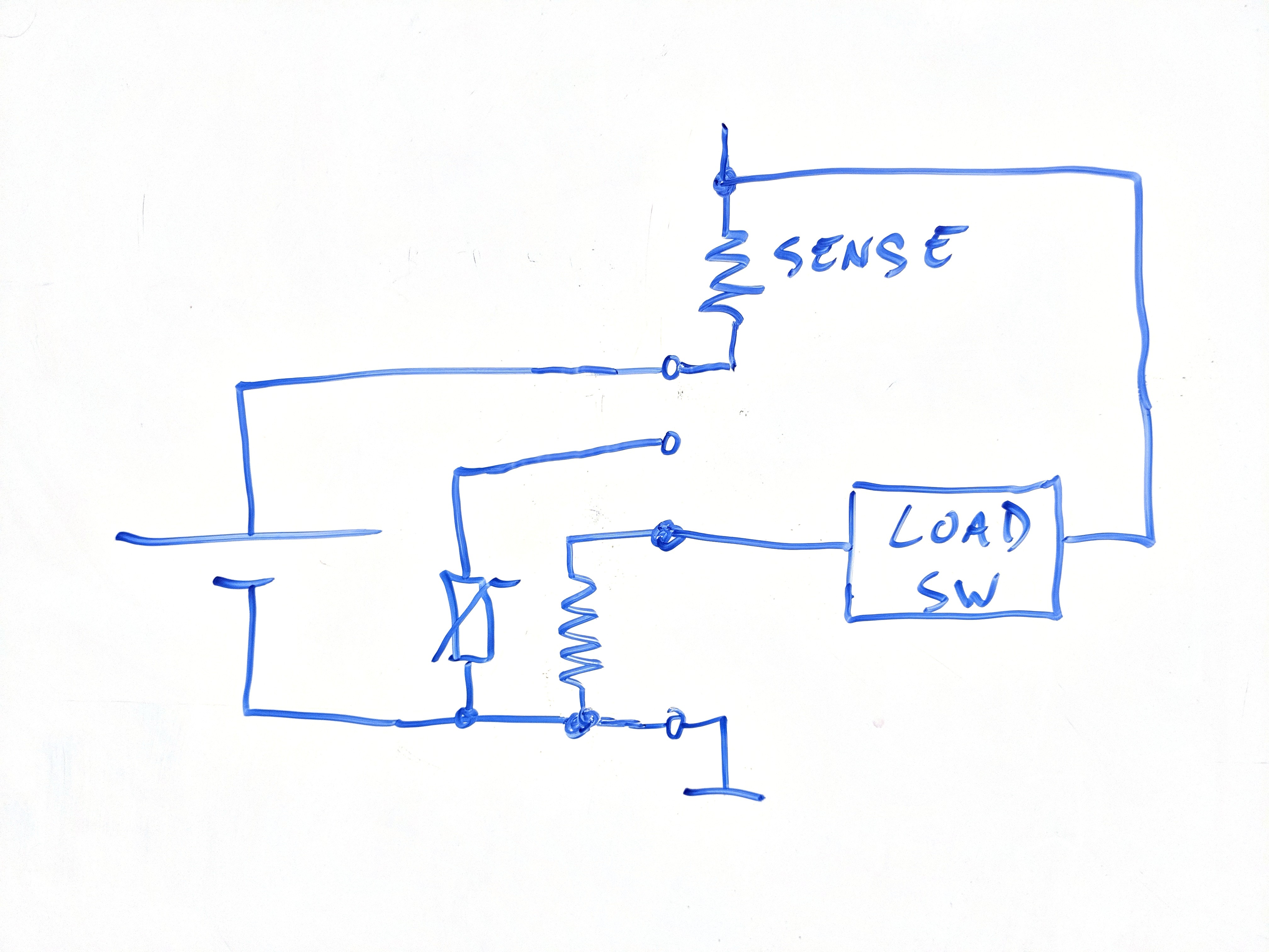
Avoiding single ended current sense measurements pretty much is the end of topology 1. However, since I now know current sense measurement near the supply voltage works well when using offset compensation, another topology (3) is possible as well: This has some advantages:
Both the thermistor and heater are now referenced to ground, making for more uniform battery pack construction and preventing another battery wire from having power on it.
Integrated load switch is preferable to MOSFET with thermal fuse. It's smaller, about the same cost and behaves better. The AP22913W6 may be a good choice at $0.14 in qty 1000 and works from 1.4 V and has a 2 A current rating.
Downside:
Battery current will now be sensed high-side, so offset compensation better work!
I will have to think about this some more, but I'm currently favoring topology 3.
 Patrick Van Oosterwijck
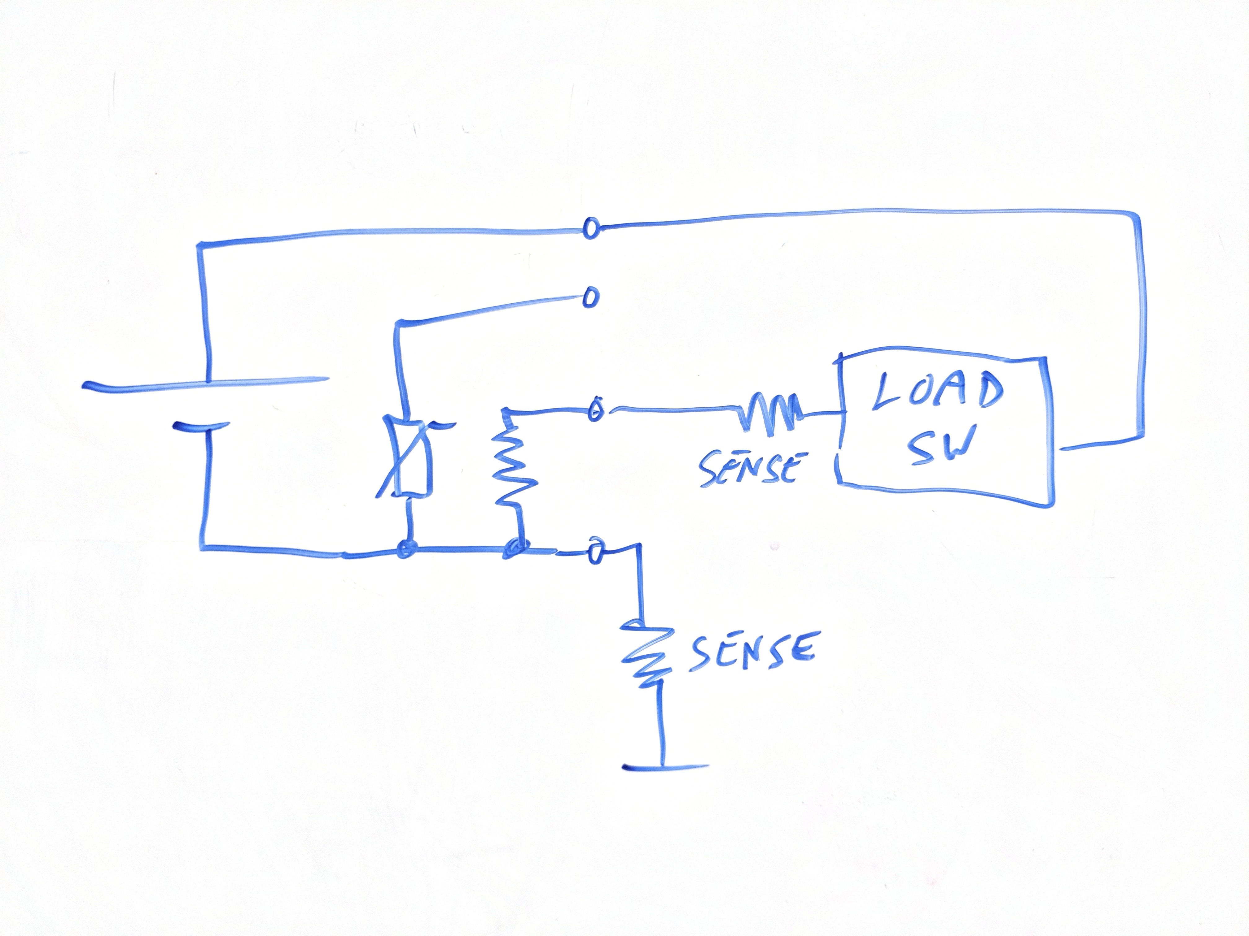
Discussions
Become a Hackaday.io Member
Create an account to leave a comment. Already have an account? Log In.