 Nicolas Schurando
I remember myself at the very beginning of the project trying to sketch on paper what the product should look like. Interestingly enough, this initial shape ended up defining a lot of aspects of the project, and in the two years that I have spent working on it, there hasn't really been a moment where I stopped and questioned whether it was the right choice.
I had already decided that it should be the approximate size of a pencil provided that I could miniaturize everything enough to fit inside. And I defined some additional requirements:
- The body should exhibit a growth that would wrap around the USB Type-C connector to alleviate mechanical stress.
- The product should be as easy as possible to assemble and disassemble. I knew given the size of the project, if I ever sold any units, I would likely be the one spending time assembling everything. And being someone who believes in the right to repair, and also - let's be honest - someone who likes to take apart everything, I wanted the end user to be able to open the product without damaging it. That meant no glue, and no screws.
For my prototypes I initially though I could get away with using 3D-printed enclosures made of two parts that would clip on together, but I would eventually always end up braking the fragile 3D-printed details after a few weeks.
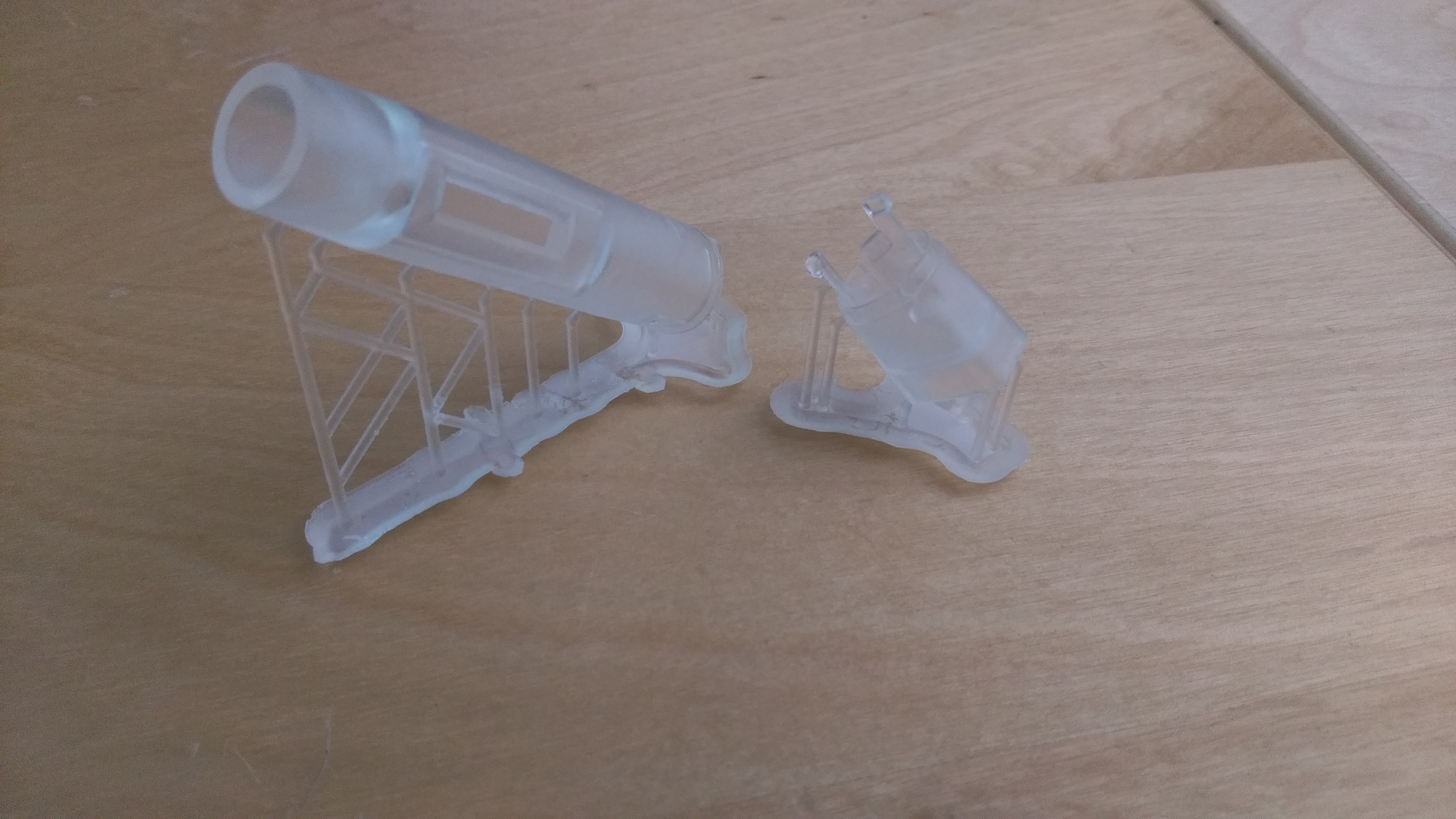
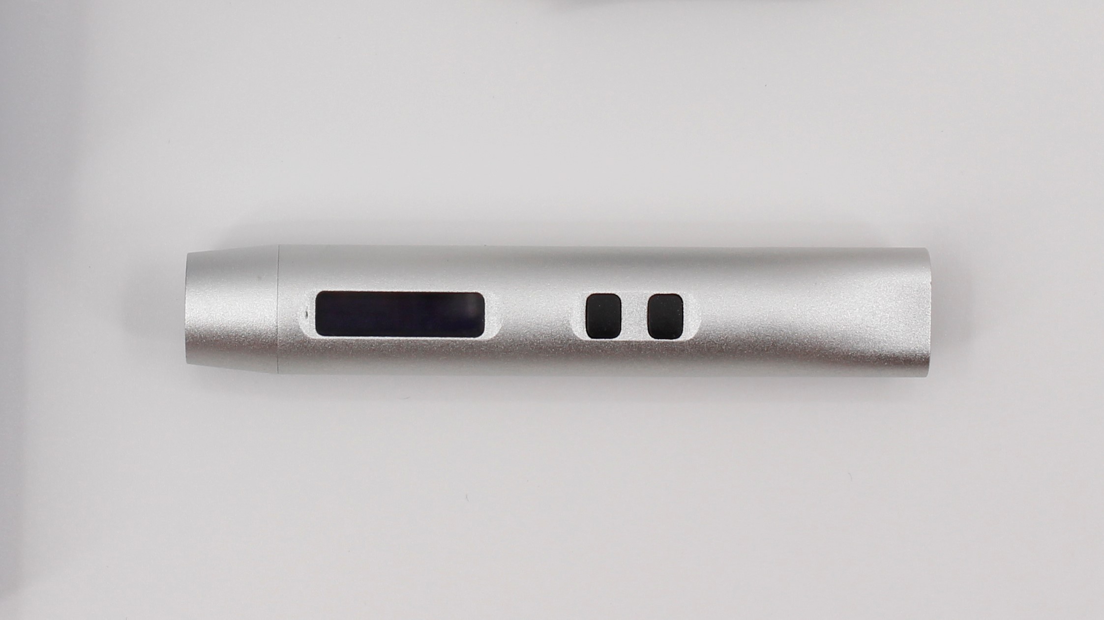
So I moved on to metal. With the initial shape being more or less cylindrical, I learnt about threads, and ordered my first CNC-machined prototypes.
I overtime eventually became more aware of what factors impact the pricing of a CNC-machined part, increased the external diameter by a couple millimeters so that it would fit in a perfect cylinder, added a nice notch for the display and buttons and voilà!
As for the inside, I faced a couple of challenges.
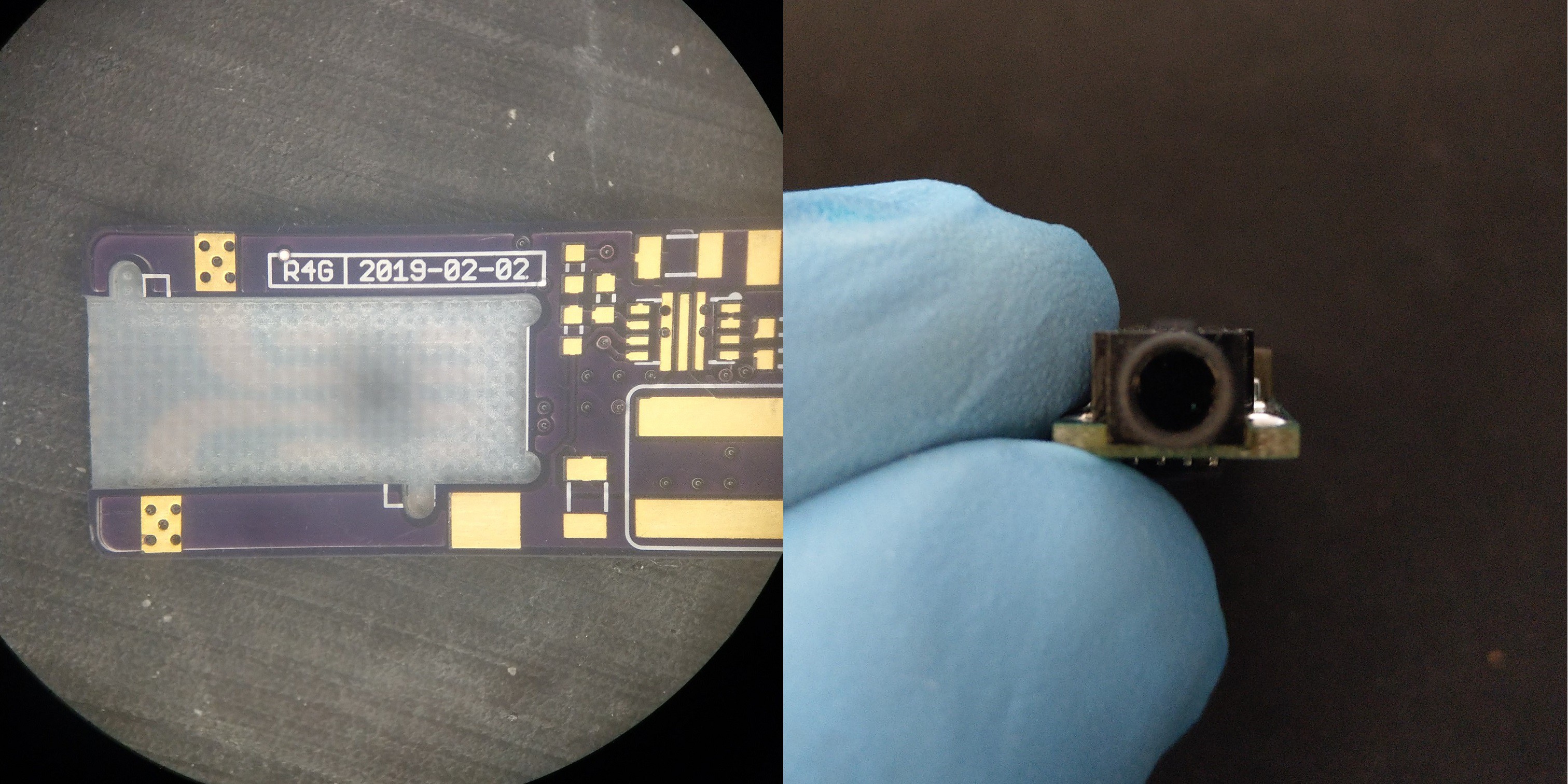
Most USB Type-C connectors are conceived for 0.8mm thick circuit boards with a double row of surface mount pins. Those two factors are a problem as 0.8mm is less mechanically resistant, and the second row being under the connector is impossible to inspect visually. Taking into account other factors, the only option left was the very expensive Würth Elektronik 632723300021. At 5 to 6 EUR a piece it was a borderline unreasonable choice, but I have to say that it performs remarkably well.
For aesthetics reasons, I wanted the jack and the USB connectors to be as aligned as possible. But with the jack connector being higher, that meant finding a mid-mount option. Which brought its own set of problems.
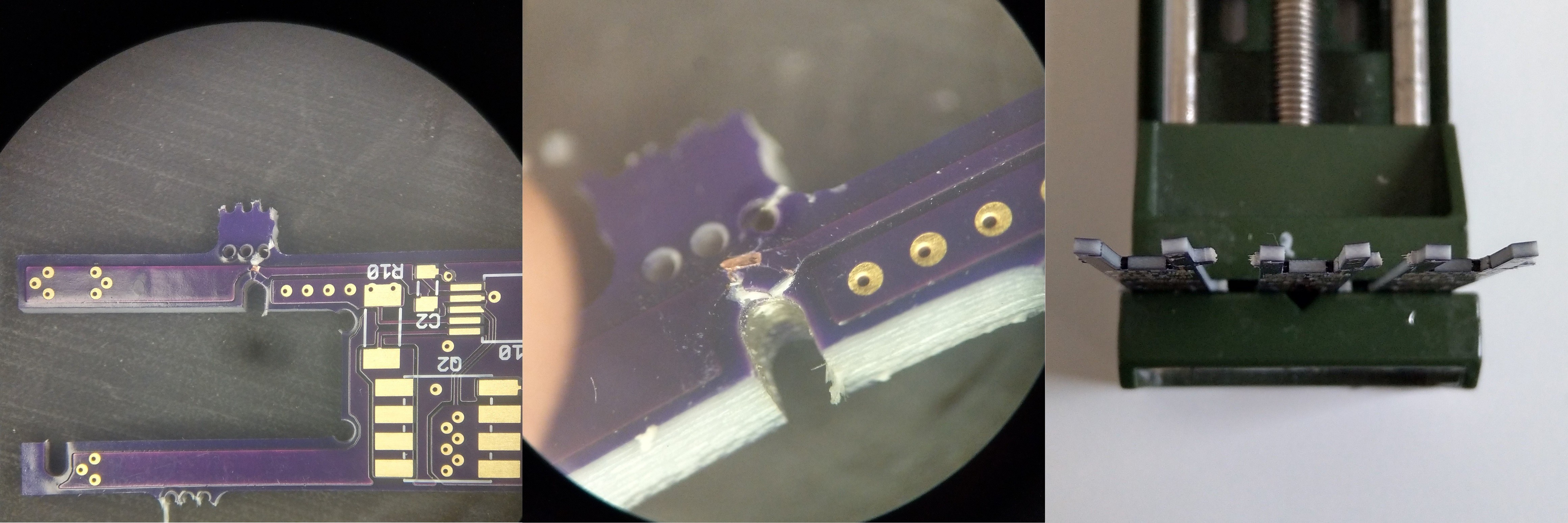
Circuit board factories place breakaway tabs in an unpredictable way that is still mysterious to me but I'm sure has to do with ensuring the structural integrity of the whole panel. As a consequence, I've had a few of my early runs fail because the separation process was putting excessive mechanical strain on a clearly too thin part of the board. Even though the amazing guys over at @oshpark have always been kind enough to redo the runs, it was clear that this was becoming a design issue. On an other note, milling trough the whole board for the mid mount connector meant less usable space on the bottom side.
So I thought why not mill only the depth necessary for the mid-mount connector?
This turned out quite well. The circuit board has better mechanical resistance, and the temperature sensing circuit is now right under the connector for better accuracy.
Discussions
Become a Hackaday.io Member
Create an account to leave a comment. Already have an account? Log In.