 Giovanni
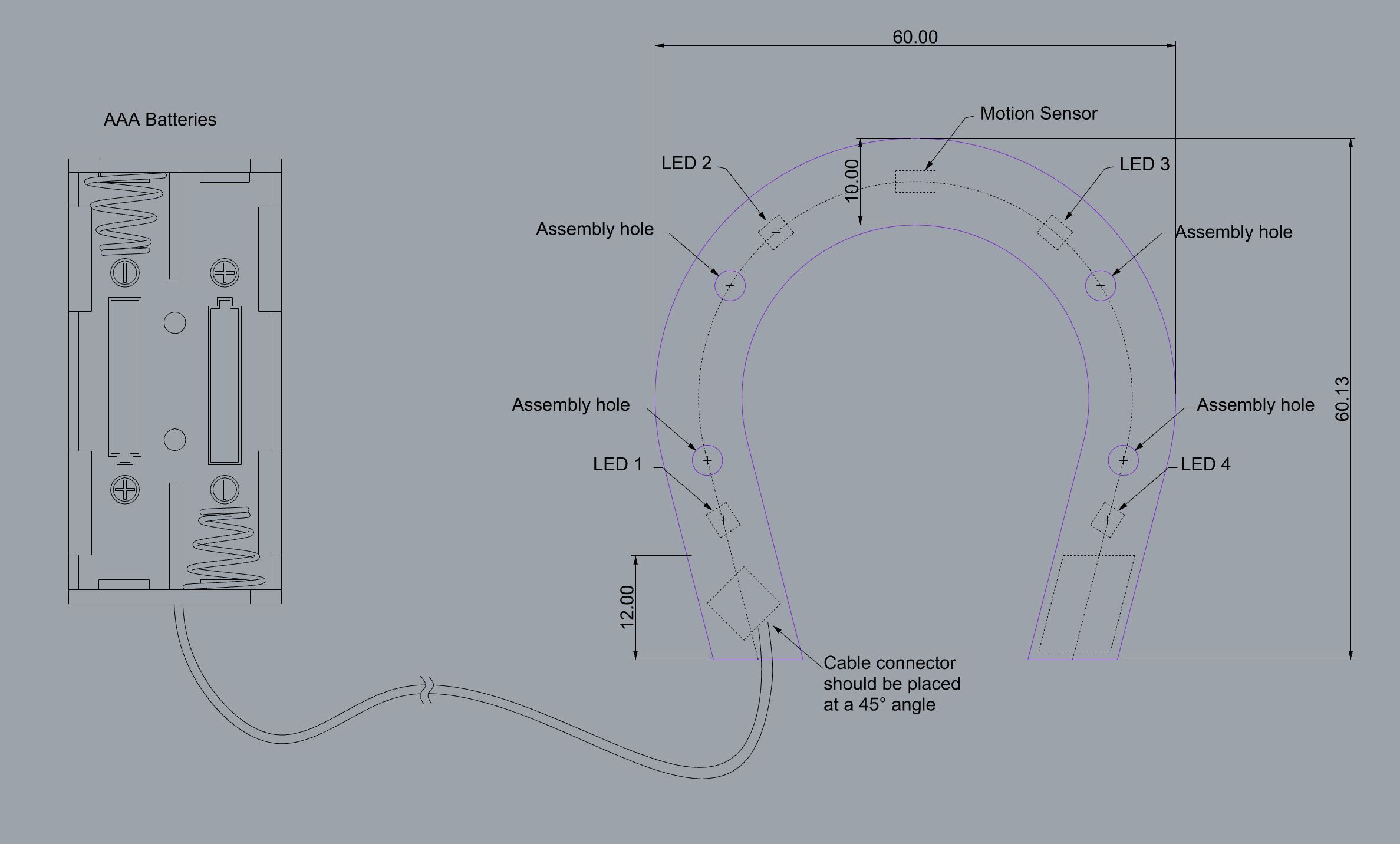 This is a very interesting part of the process because here is where electronic engineers and product designers finally butt heads.
Based on the design of the lamp, I shared with Voja a sketch with the ideal location of certain components on the PCB. I am not an electronic engineer, so there are many components I do not know we need and/or their location, therefore I try to keep my communication simple, detailing:
- Basic shape or outline and assembly holes
- Location of input/output components (LED's, connectors, power source, etc)
- Other restrictions or requirements (light pipes, etc)
- Everything else I assume is going to be populated with a bunch of resistors, capacitors, micro controllers, etc.
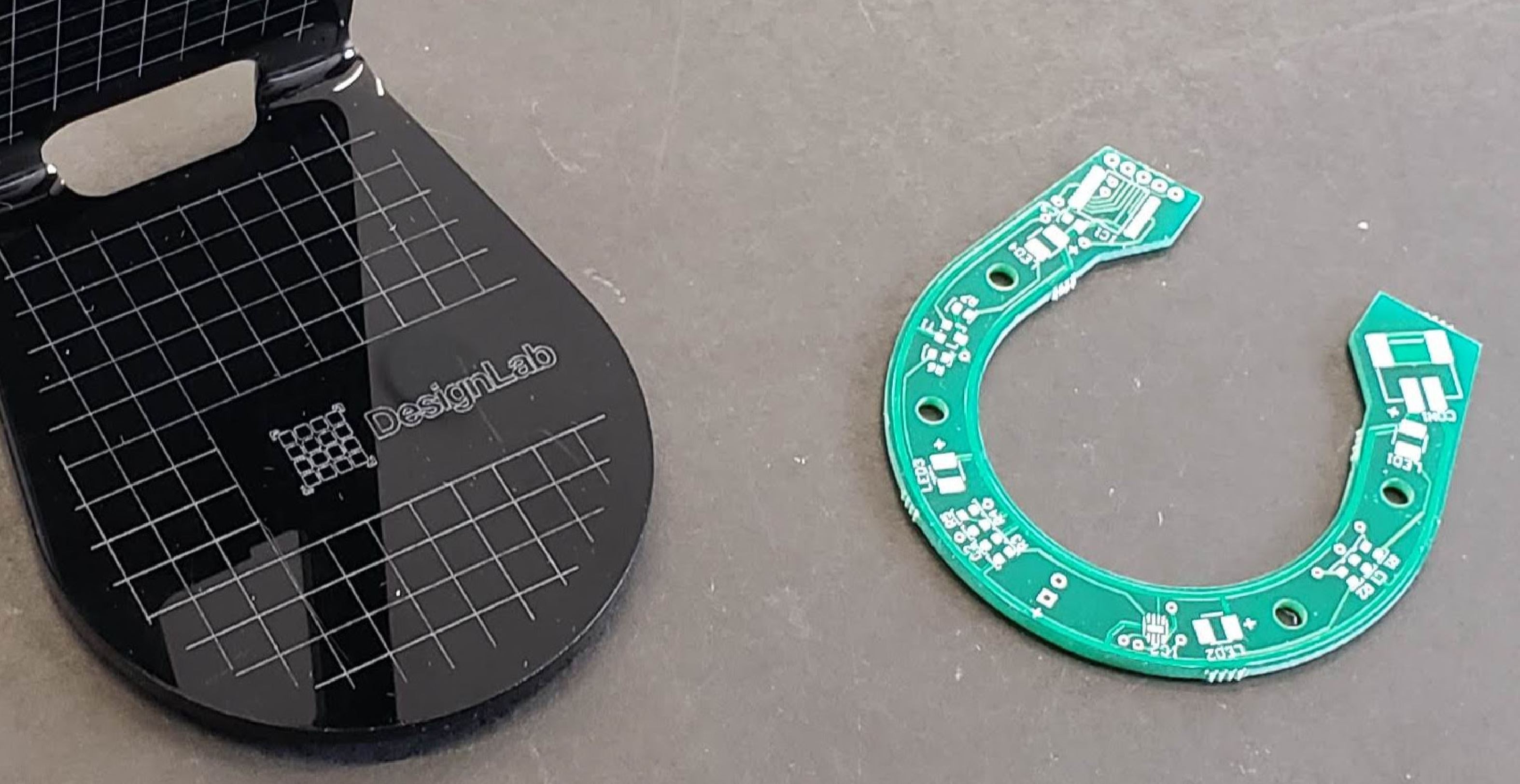
The electronic engineer (or yourself) might come back to you with further requirements, requests for more space, different orientations, etc. This is where the fun begins. Fortunately, this is a rather simple project so Voja managed to skillfully fit everything on a single board. Once that was confirmed, time to go back to the 3D model to update component location.
Discussions
Become a Hackaday.io Member
Create an account to leave a comment. Already have an account? Log In.