 Giovanni
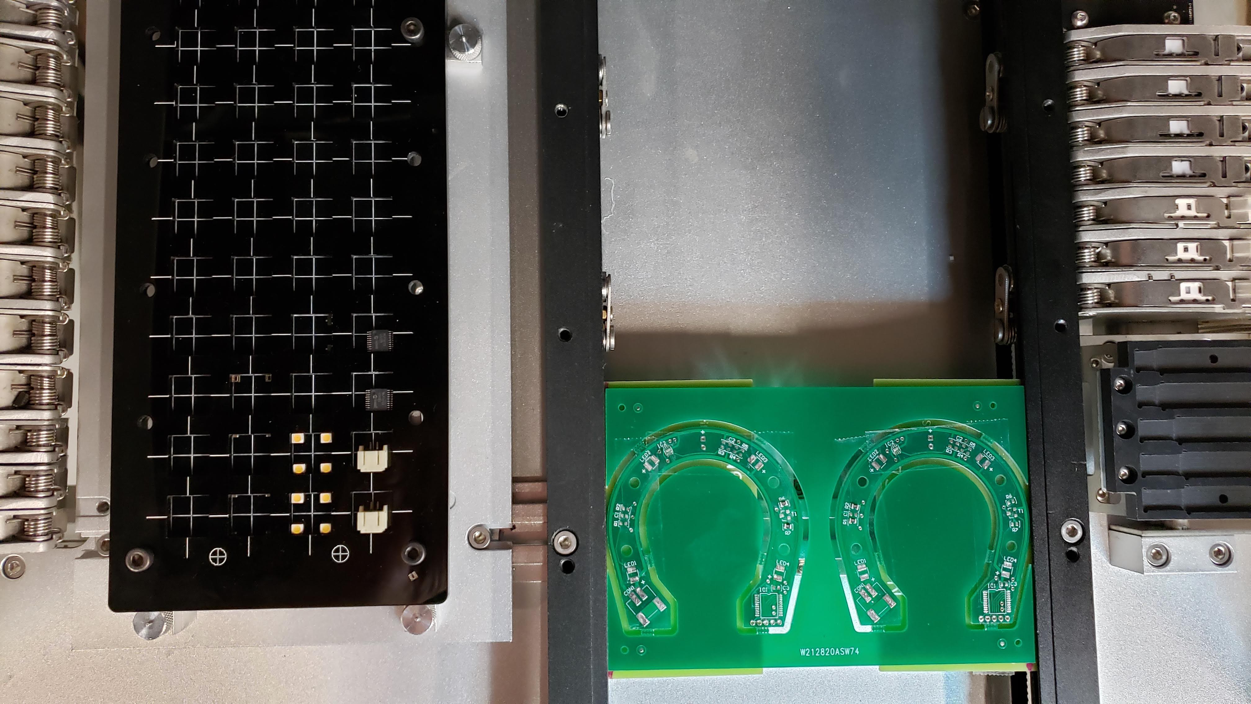
The first PCB panels we received had a minor but fatal flaw: no extra spacing to the sides, meaning that rails ended up blocking some of the traces.
Erika improvised adapted and overcame the challenge by adding extra material to the sides in order to get us those badly needed 5 mm. Of course, this is a temporary fix and I just ordered new, improved boards today.
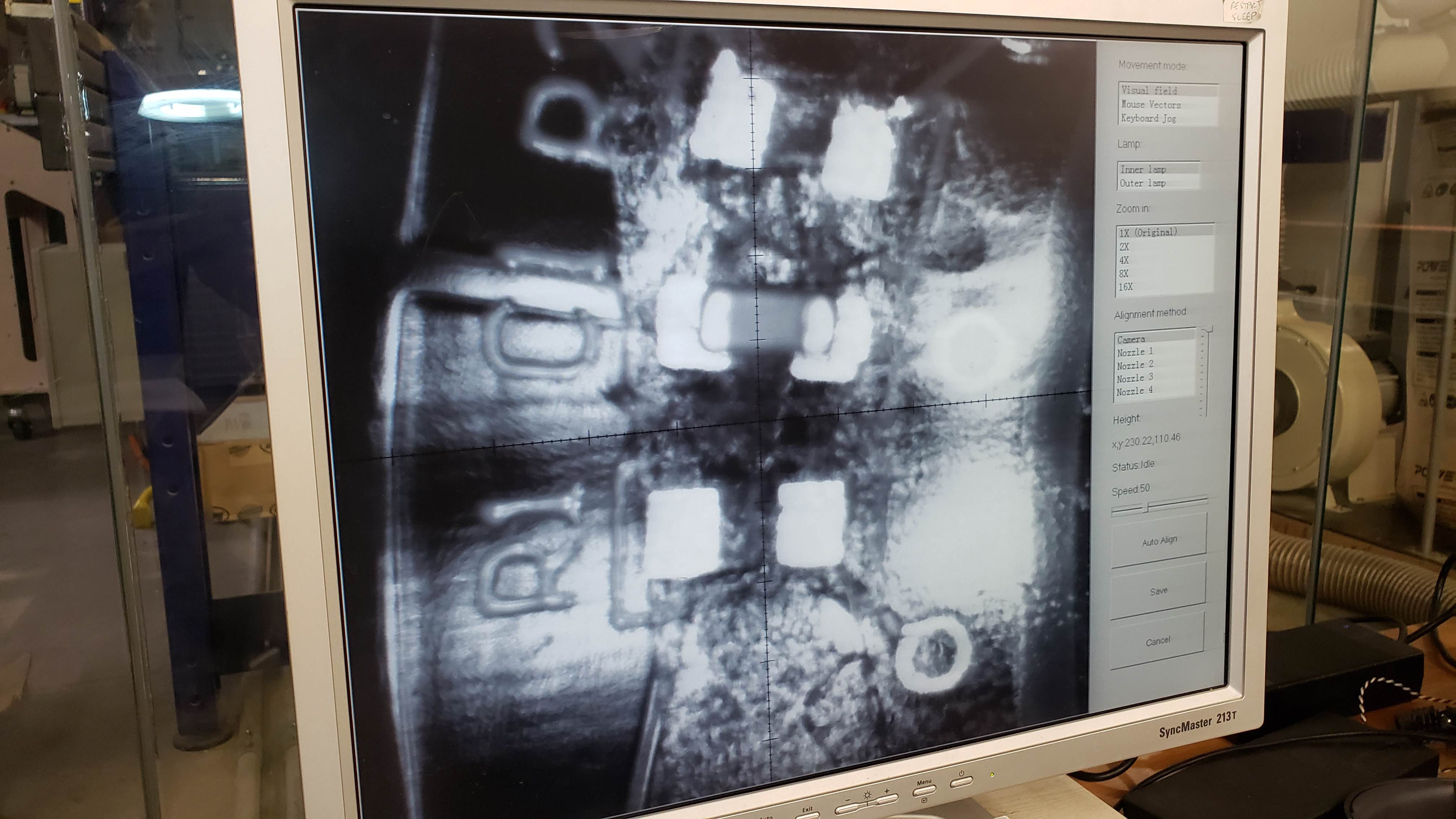
 The precision on these machines is very good. The cycle to pick a component and place it on the board has quite a few steps that I am unable to describe, but Erika would in a heartbeat. Essentially, the machine takes photos of the nozzle (?), board fiducials, grabs component, goes for another selfie and then flies over to the exact location where such component should be placed.
This photo was taken by the machine after it placed that resistor on C1. See how well centered the component is on the board? Now check out the next photo for a better idea of the scale.
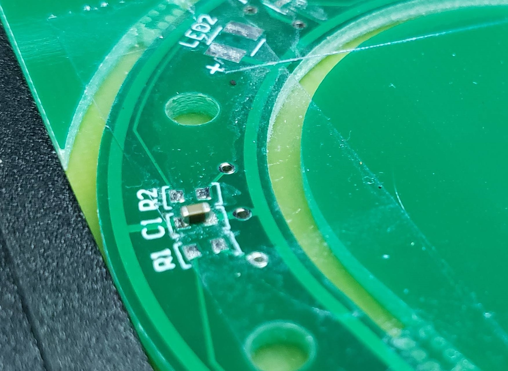
Pretty crazy, uh?
Want to see the Pick and Place in action? Grab your popcorn for an awesome 17-second video with the sequence I eloquently described above.
Discussions
Become a Hackaday.io Member
Create an account to leave a comment. Already have an account? Log In.