 land-boards.com
I bought a bunch of Z80 parts on ebay for cheap ($10 plus shipping). The parts came on a PCB which had not yet been flow soldered. From the date codes of the parts it looks like it was stuffed sometime around 1999. All I had to do was straighten some pins which were bent over to hold the parts in.
Here's the parts pulled from the card.
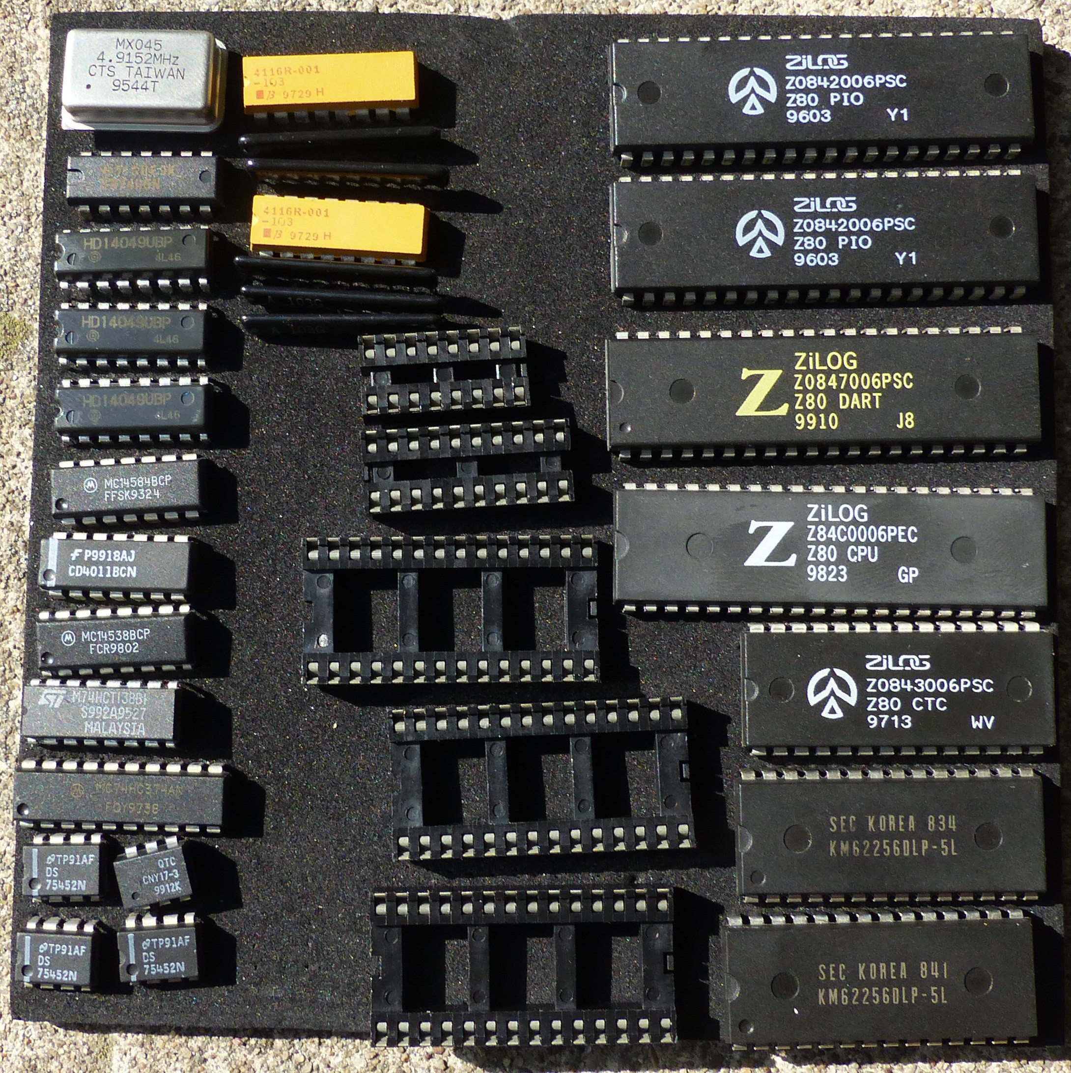
The parts included:
- (1) Z80 CPU @ 6 MHz
- (2) 32KB SRAMs
- (2) Z8420 Parallel I/O (PIO)
- (1) Z8430 Counter Timer Chip (CTS)
- (1) Z8470 Dual UART (DART)
The parts are all 6 MHz rated.
The only thing that is missing is an EPROM and glue logic. I will use an EEPROM so that it can be updated easily.
I want to build a retro Z80 CPU using these parts. I've already done a bunch of retro CPUs using the venerable Multicomp project by Grant Searle inside an FPGA. But I'm itching to build the "real thing" with these discrete parts.
Searching for 5V Glue Logic
I need glue logic to hook the parts up together. There are few options available nowadays for 5V glue logic. Nearly everything "out there" runs off 3.3V. Sure I could throw down a bunch of 74LSXX gates and that would work just fine. But I've gotten used to the flexibility that comes with programmable logic and I don't want a bunch of configuration jumpers. And I'm not yet sure what software I want to run so figuring out the details of the Peripheral Memory map would be a pain at the start. Plus, the ability to switch out the EPROM and run out of SRAM will introduce another bit of logic.
Picking the Glue Logic
I've done a few projects before using the Cypress Semiconductor PSoC5LP. It's a handy 32-bit ARM CPU that is not too expensive (under $10 in qty 1 pricing). It comes in a 100 pin TQFP which isn't too hard to solder (I have to use a microscope). And it runs at 5V with plenty of I/O.
But, why use a PSoC as "glue" logic?
Because the PSoC is an odd beast. It combines an ARM CPU and a programmable logic area. Sure there's FPGAs out there with ARM cores. But this is different. It's more of an ARM CPU with programmable logic than a big and expensive FPGA which also has an ARM core.
The logic area on the part isn't too big. But it isn't too small either. It should be big enough to hold the glue logic for a Z80 microcomputer. Having an ARM core inside the part is just a nice bonus. Never mind the fact that the ARM core is much more powerful than the Z80. This is about retrocomputing but there's no reason the glue logic can't be re-imagined for the 21st century.
Programming the PSoC
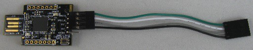
The programmer for the PSoC is really cheap in the form of a $15 development board which has the USB - SWD programmer and a sample target design. The programmer/dev board is part number CY8CKIT-059 and is available on Mouser. Here's the programmer itself. It only requires a 4 pin header to program the PSOC. Unless you are right next to your USB hub you'll also need a USB A:A male-female cable to get to it.
Pretty simple to use. It requires installation of the PSOC Creator but the programming is all in C/C++ so it's pretty standard stuff. Plus, there's a nice schematic editor for the glue logic part.
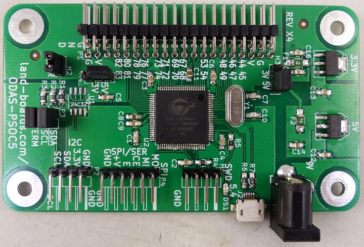
A while back I made a stand-alone board with the PSoC5 LP on it and will use it for a proof-of-concept.
Features
This concept opens up a lot of possibilities. There are tons of I/O on the 100-pin TQFP part. The Z80 CPU could be halted (or held in reset) and the EEPROM could be programmed from the PSOC. Heck, the EEPROM could even be eliminated and the program loaded from the PSoC into SRAM and run after downloading.
Besides the glue logic there are all the usual peripherals in the PSOC (USB interface, Serial ports, I2C, SPI interfaces, etc). These could come in handy with a card like this.
Picking the PSoC Part
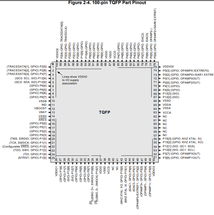
There are quite a few parts available in the Cypress Semiconductor PSoC family. I used one of the less expensive parts, the CY8C5267AXI-LP051 before (it is $8.67 on Mouser). This part compares well to the $5+ for the obsolete EPM7064 on ebay. And I won't need a socket for the PLCC CPLD. The downside is that it's a surface mount part with fine pitch. It's also pretty small. But I've soldered quite a few of these when people got them on my Kickstarter.
Schematic Design
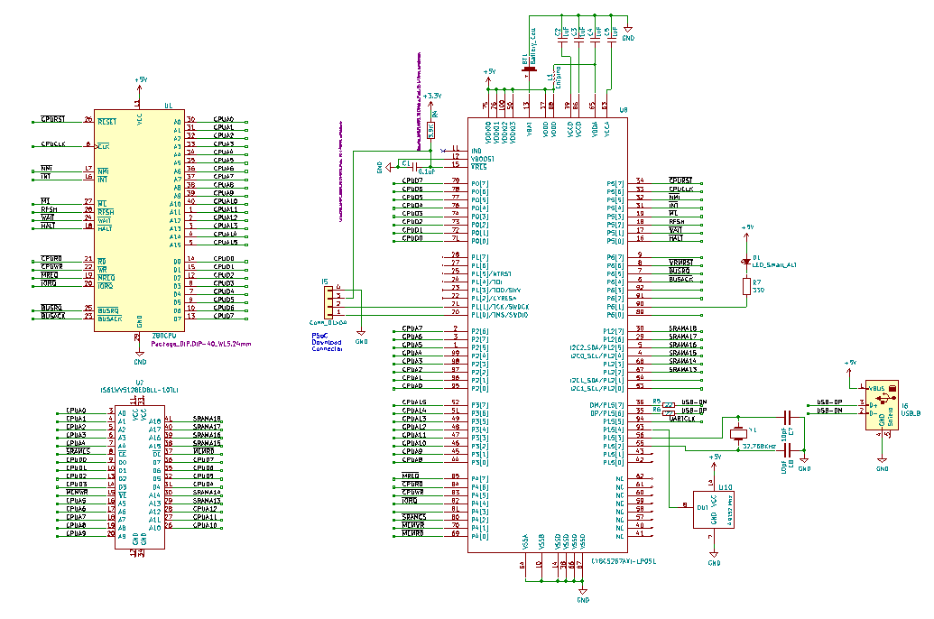
I fished around on the web for the KiCad symbols for the parts that I needed to use for the board design. They are not in the standard KiCad libraries - probably too ancient for most people. I found them all. Plus I already have the symbol for the PSoC. Here's a very rough cut at all of the parts thrown down onto a schematic (link to GitHub).
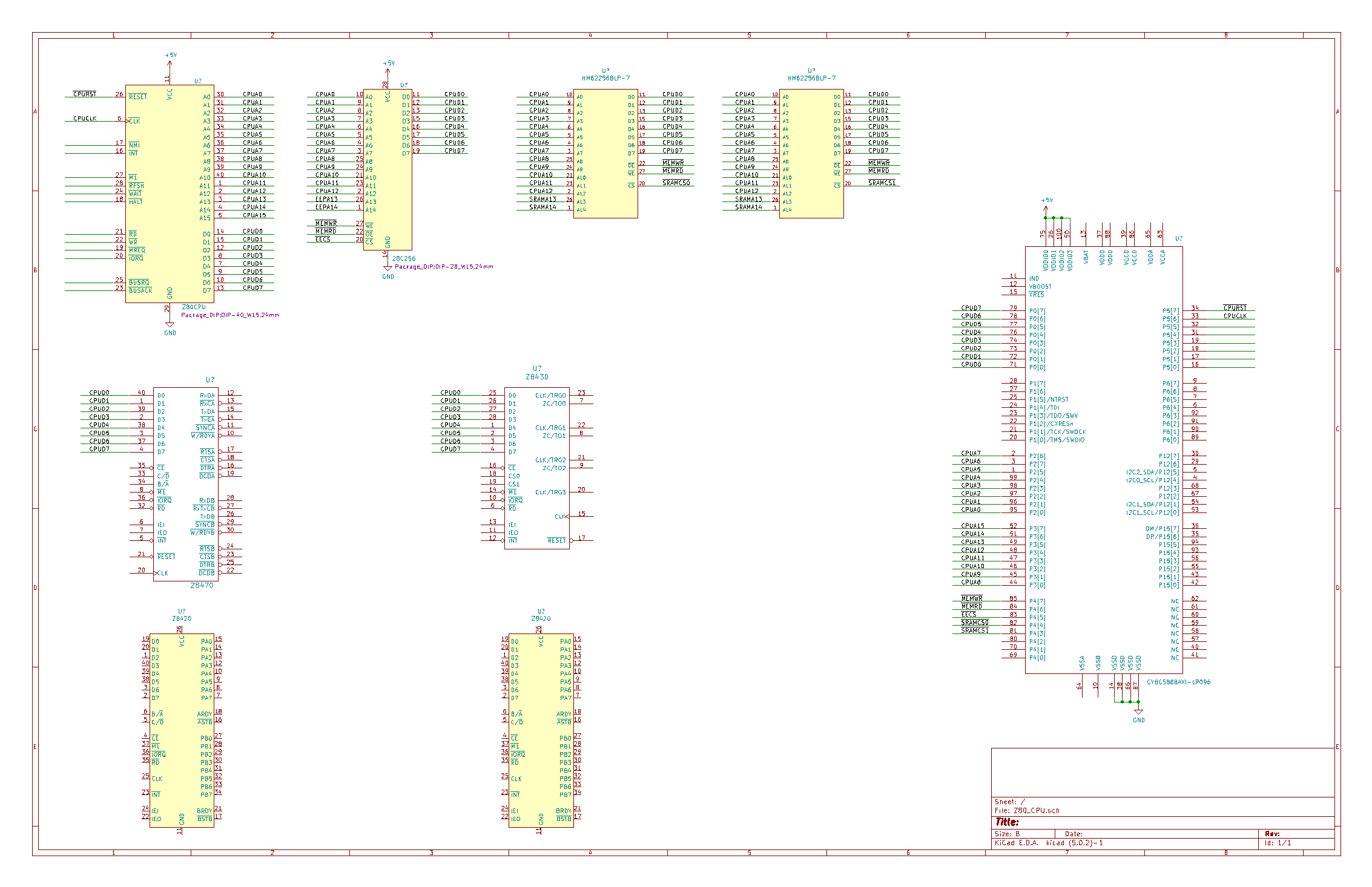
All of the Z80 related parts (Z80 CPU, DUART, CTC, 2xPIOs, 2x32KB SRAMs) came with the unstuffed Z80 CPU card. The EEPROM and PSoC part will need to be purchased.
Design Details
There should be plenty of I/O to even connect all of the address/data lines from the CPU directly to the PSoC and still have enough control lines to generate the control signals for the Z80 parts. This might be tight. Many of the control lines might not need to go through the FPGA. The key feature is EEPROM programming and that takes nearly all of the address lines and all of the data lines plus control lines.
Downloading the EEPROM
I definitely don't want to mess with figuring out how the program the EEPROM with an external programmer. The PSoC is more than capable of performing the task of programming an EEPROM. I figure that the PSoC needs to get the bus from the Z80 via BUSRQ* and wait for BUSACK*. Then, it needs to drive the three control lines (MEMWR*, MEMRD* and EECS*) along with the address bus (CPUA[0..14]) and data bus (CPUD[0..7]). This should make for a fairly easy code development cycle.
Measuring PSoC I/O Latency
The first thing I want to figure out is the I/O latency on the PSoC. For this I will generate a clock on an output pin and route the clock back into the part. I will then send it through an OR gate and out a pin. This should be a decent test of I/O and logic latency in the PSoC. This shouldn't be a challenge for the PSoC logic since it's competing against 74LSxx series parts (often in a couple of stages) for speed.
Here's the schematic for the clock output:
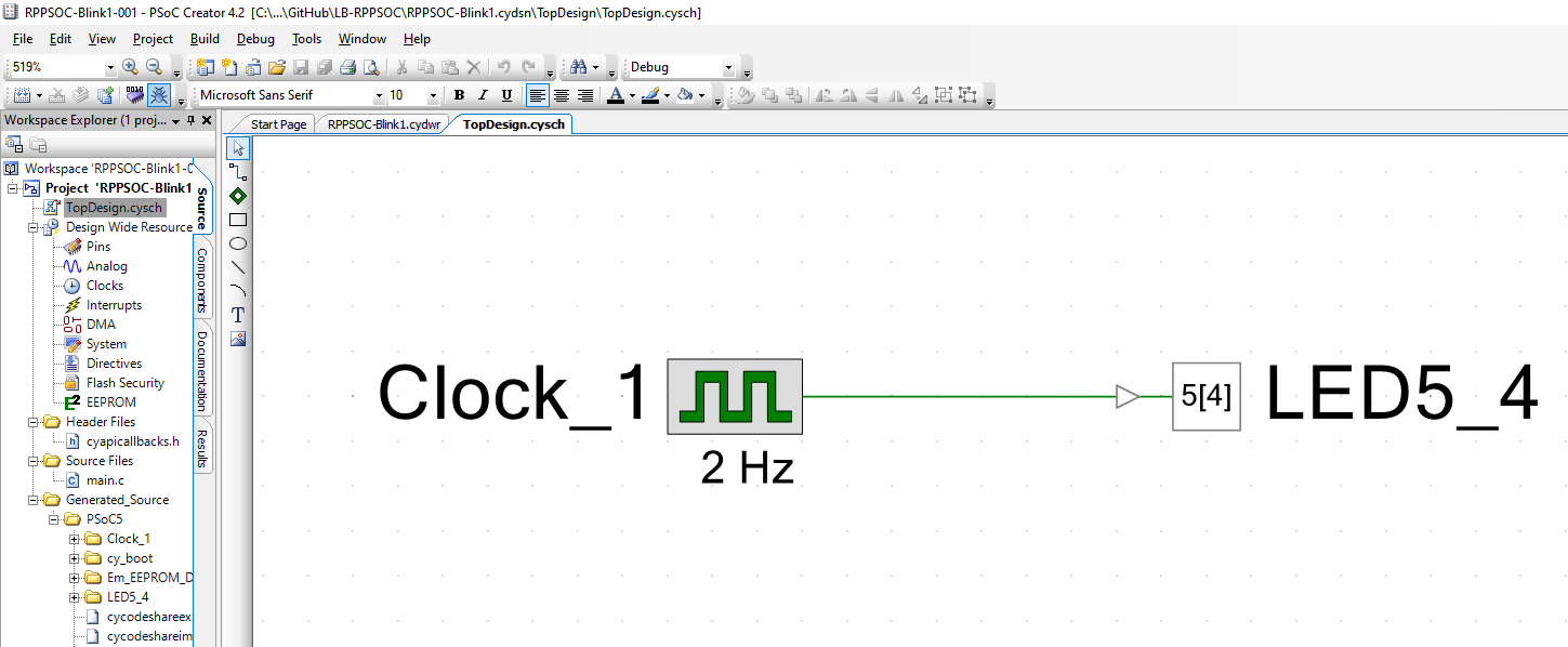
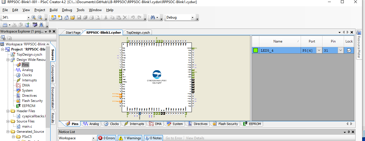
Pretty simple, right? All it does is generate a 2 Hz clock on output pin 5[4]. The PSoC pinout is:
Testing on PSOC Card
Pin 5[4] is Pin 31 which is on an LED on our ODAS-PSOC5 card (located near the Mini-USB connector).
The light is flashing after downloading (select the port with Debug | Select Target and Program the Acquire the part and download). It's been a while since I've programmed the card and I forgot just how easy it us to develop code for the PSoC on this card. All it takes is a 9V power supply since the card generates the 5V needed to power the I/O and CPU core.
Changing the output pin to Pin 83 which is near the bottom of the board is simple, too. Pin 83 is Port 4[5] (confusingly similar, huh)? Double click on the Pins and up pops the pin planner. Change it to Port 4[5], hook up an external LED and build/download. Took less than 15 seconds to compile/download and the LED is blinking on the external pin.
I put an archive of the PSoC files in my Retro-Computing repository on GitHub.
It would make sense to add an LED to the schematic at this point. It's a good way to know the PSoC is up and running. Easy enough to do it as I go along. I'll probably put it somewhere else but this is a good way to remember to do it.
Now it is time to measure the PSoC latency. To do that add a couple of pins, two ins, one out. Add an OR gate to make sure the signal actually goes through some minimal internal logic and doesn't just connect an input pin to an output pin. To add a pin, go into the Component Catalog and select Digital Input Pin. Drag it onto the schematic. Name it IN1. Repeat for IN2 and then make an output pin the same way. The OR gate comes out of the component catalog under Logic and by selecting OR.
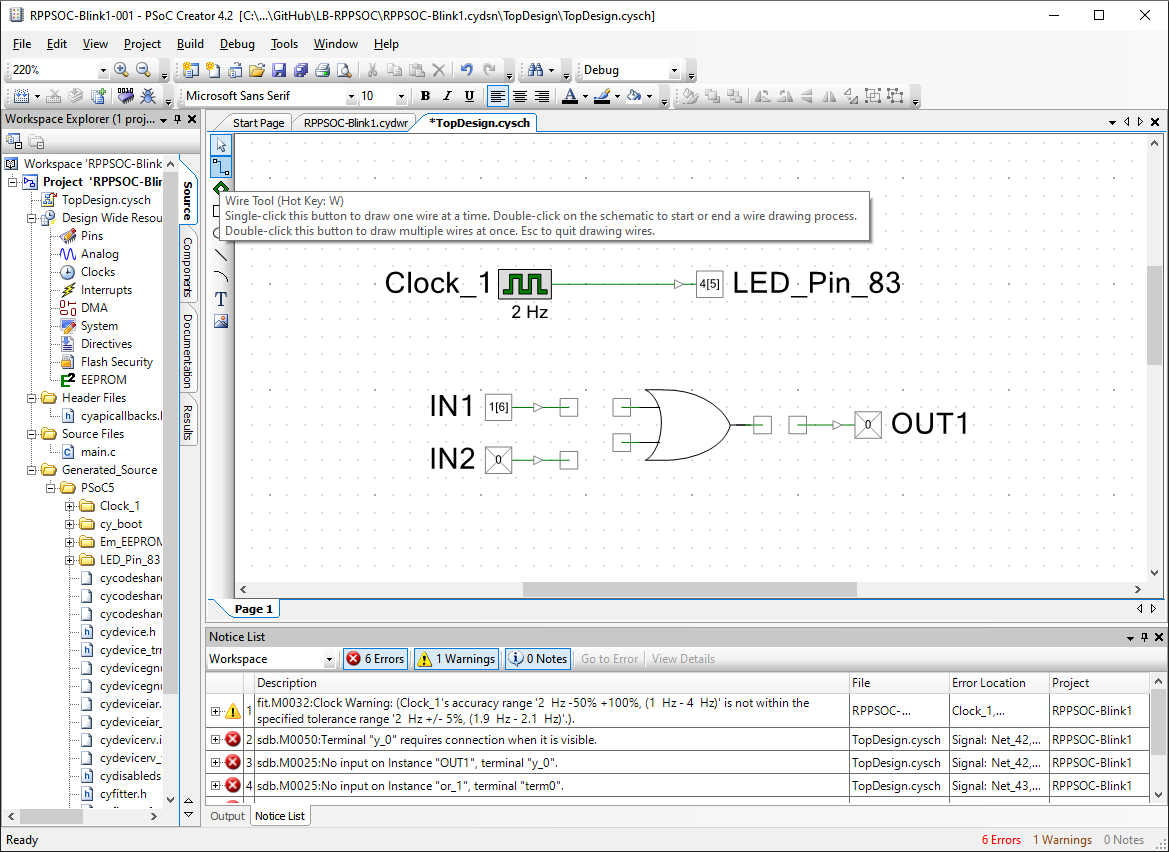
To connect the pins, use the Wire tool. Don't confuse it with the line drawing tool which doesn't connect stuff. One of the very nice things is that the bottom of the screen in the Notice List shows DRC errors as you go along. For instance, after hooking up the two input pins, if the OUT1 is not connected, it warns that the pin and output of the gate are not yet connected:
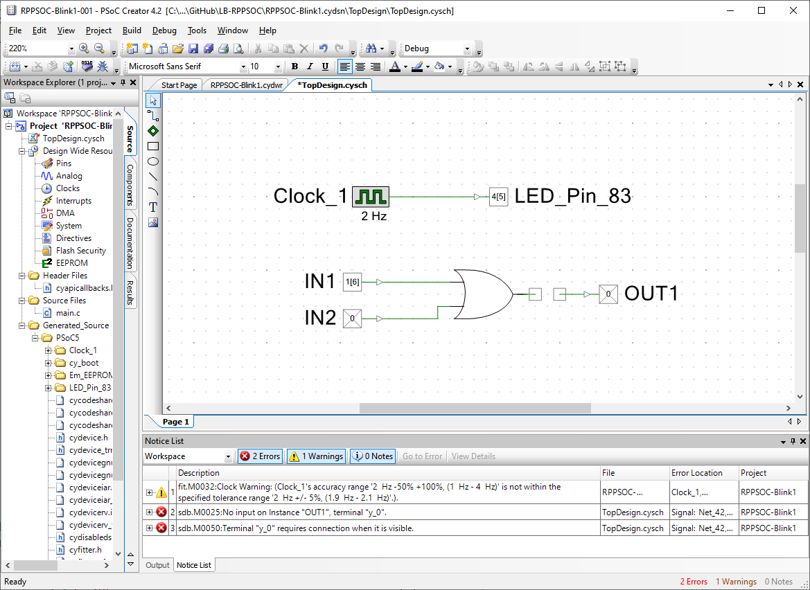
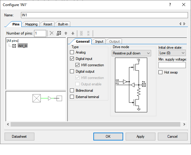
One of the nice things about the PSoC is that you can assign a lot of configuration values to the pins by double clicking on the pin. For this OR-gate, I want the input pins to have resistive pull-downs and the part support that easily. Go to Drive mode and select Resistive pull-down.
 I assigned the I/O pins as follows:
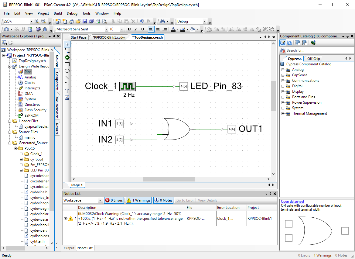
This puts the pins on the I/O connector next to the LED_Pin_83 so that I can jumper from the 2 Hz output on Pin 83 to one of the OR-gate inputs on Pin 81 with a shunt. To check, the LED gets moved to 4[4] which is pin Pin 82. The other pin (Pin 80) is already pulled-down with the resistive pull-down so it can be left floating.
Changing the I/O pins is easy. Just pick new ones. And I did since it was "hard" to get to the output pin. Changed them to:
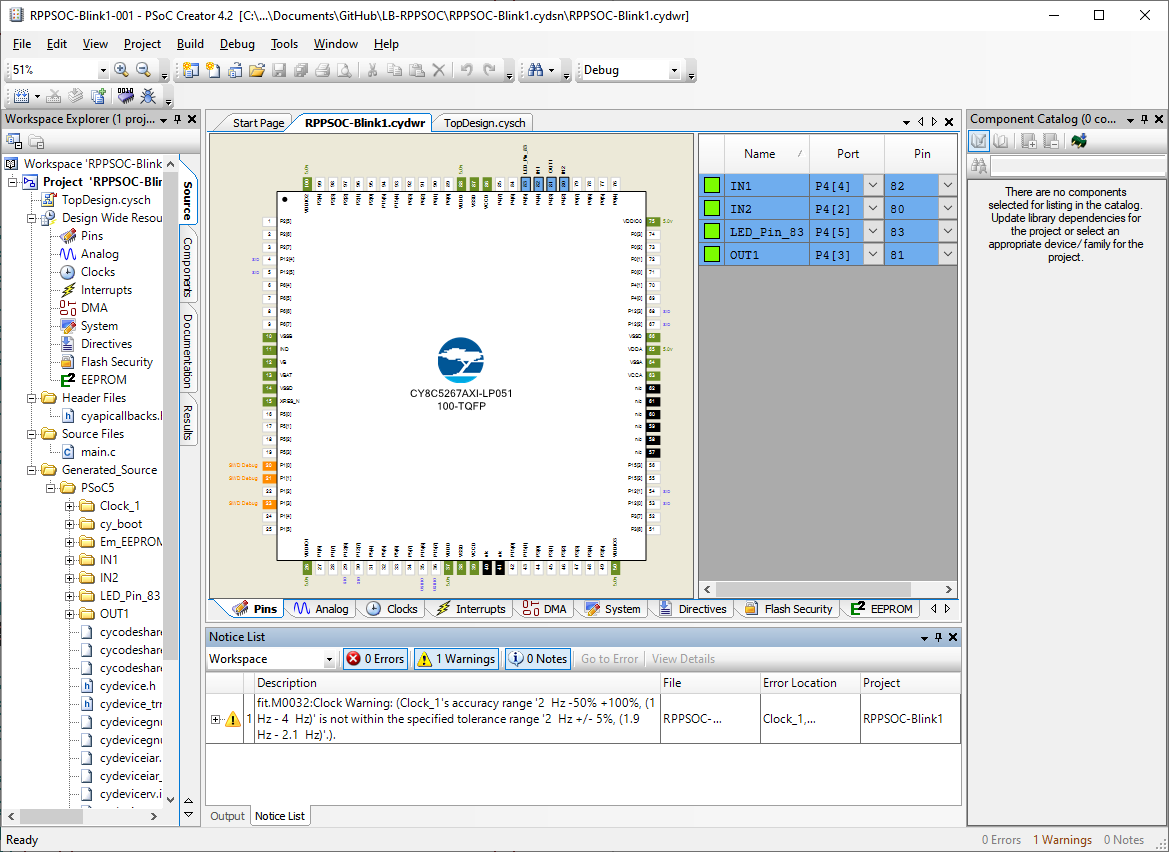
Moved the LED output to OR input using a shunt to connect pins 82 and 83. Ran and the light is now blinking on pin 81. And I can get to the pins with the scope to measure the latency.
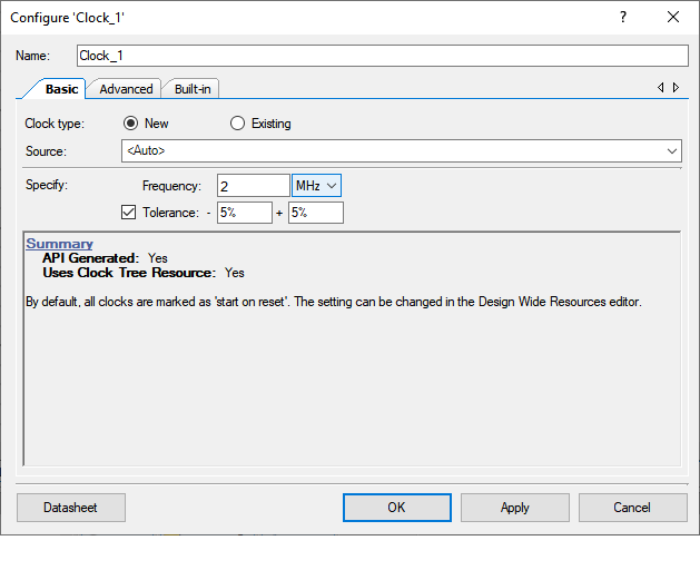
Even with a storage scope only having a clock every second strains the ability to get a good measurement. No problem, it's easy enough to change the clock output to a higher frequency. Just double click on the Clock_1 pin and change to MHz.
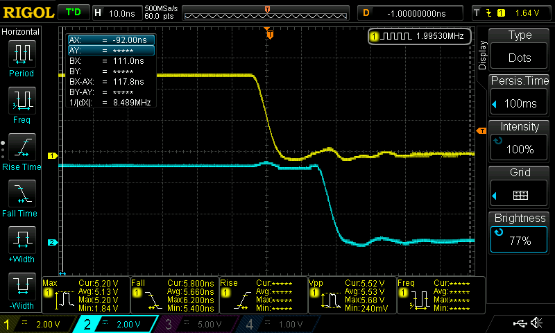
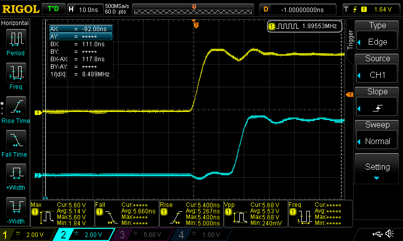
Here's the High-to-Low output propagation time captured on my DS1054Z scope. The propagation delay is less than 20 nS. Not blazingly fast, but not too bad. I don't anticipate extra layers of logic adding much but I'll have to measure to be sure.
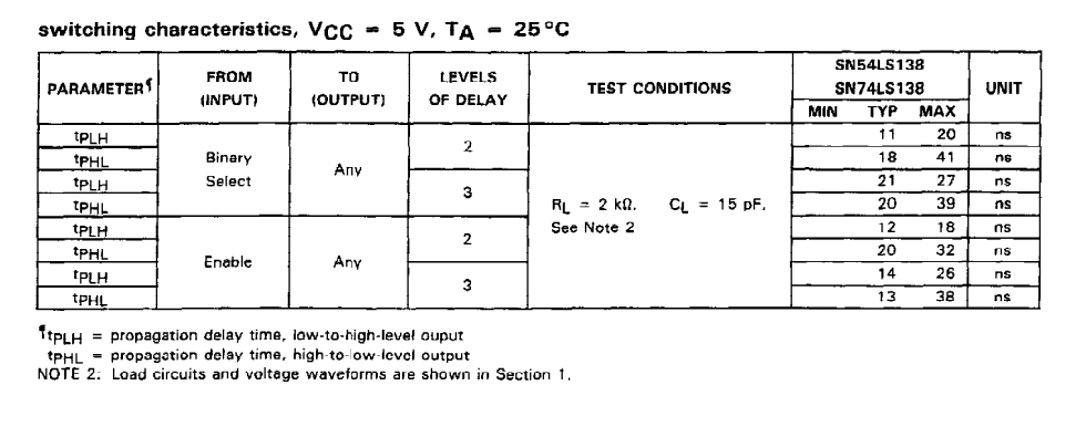
Compared with a 74LS138 often used as an address decoder, it's close to the specified typical times and certainly faster than the worst case maximum time.
The Low-to-High output propagation time is slightly faster (17 nS). Here it is as captured on the scope:
Comparing this speed vs an established discrete design points to performance advantages of this approach. Here's the I/O chip select logic from the Zeta SBC 2 board (the design is for an 8 MHz CPU and my design is 6 MHz):
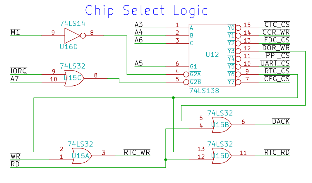
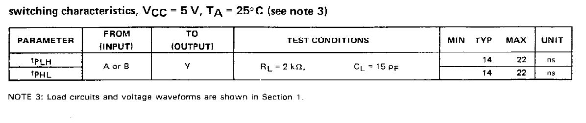
IORQ* goes through U15C (a 74LS32), through the enable lines of U12 (74LS138) and out to most of the chip selects. The RTC_RD* has an extra delay. through U15D (74LS32). The LS32 spec shows a typical propagation delay of 14 nS:
Looks like the PSoC logic should be fast enough.
Real Time Clock
There is a real time clock on many of these cards to keep system time. There's the possibility of using the battery pin on the PSoC and some internal counters to provide a battery backed up clock. The PSoC datasheet says:
Sleep mode is optimized to provide timed sleep intervals and
Real Time Clock functionality.
Sounds like that is a possibility. The Cypress datasheet for the Real Time Clock says:
The Real-Time Clock (RTC) component provides accurate time and
date information for the system. The time and date are updated
every second based on a one pulse per second interrupt from a
32.768-kHz crystal. Clock accuracy is based on the crystal
provided and is typically 20 ppm.

PSoC supports a wide range of low-power modes. These include
a 300 nA hibernate mode with RAM retention and a 2-µA sleep
mode with RTC. In the second mode the optional 32.768-kHz
watch crystal runs continuously and maintains an accurate RTC.
I may need to emulate the common DS1307 Real Time Clock inside the PSoC. That sounds like a good sub-project for later on.
For now, I'll just put on a 32.768 KHz crystal on the schematic. Cypress Application Note (AN54439 - PSoC® 3 and PSoC 5LP External Crystal Oscillators) covers this operation. The PSoC datasheet shows the connections required.
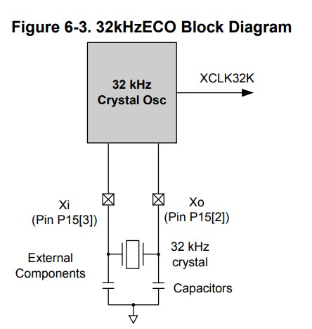
The application note says that the capacitors should provide the proper load for the watch crystal selected. For now, I'll toss on 10pF for placeholders at pins 15[2] and 15[3]. It's easier to install the parts and not need them than not have the pads.
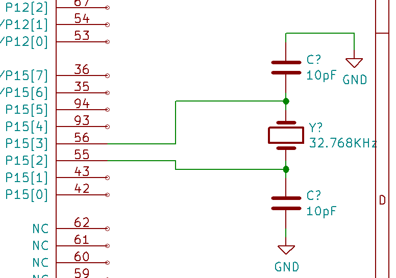
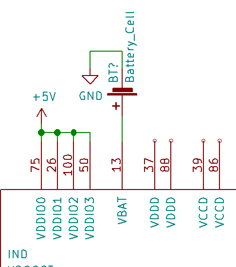
While I'm thinking about it, time to connect a Coin Cell battery to the VBAT pin on the PSOC to power the RTC.
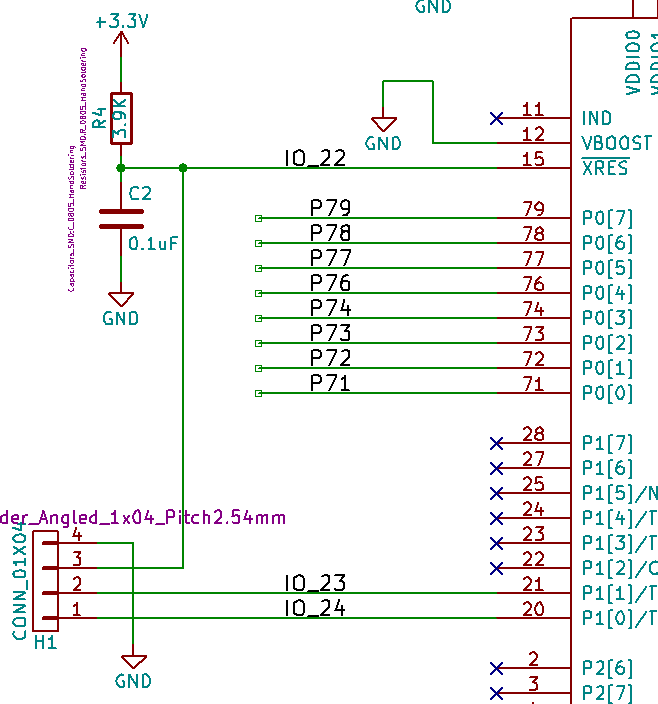
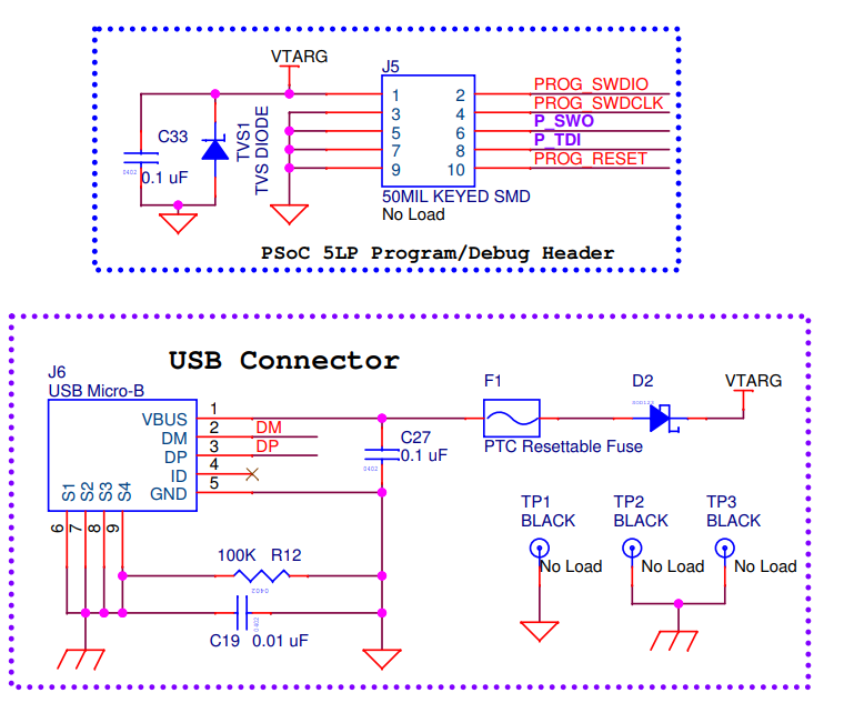
PSoC Download Cable and Reset
While we are on the datasheet, let's add the download cable and reset circuit. I've used these before so they should be fine for this design. The connection from the PSOC programming header (H1) to the reset line allows the PSOC to be reset by the programmer. The PSoC has a complex reset circuit with voltage monitoring, etc, but it seems to be OK with just a 0.1uF cap to ground. The pull-up may not be needed since XRES* is pulled-up inside the part but this make sure it goes high.
Power and USB to Serial
I like using USB cables for power. In fact, I like using old school USB A:B cables for 5V power. The big old B connectors feel more solid than the mini or micro cables. And they are through hole. Cheap, too, at $0.65 from mouser. A lot less painful to hand solder than the surface mount mini or micro connectors. The USB controller in the PSoC has its own internal 3.3V regulator so using 5V on the other I/O pins shouldn't be a problem.
The connections for USB are pretty simple (from the datasheet):
One "free" bonus of connecting up USB for power is that the PSoC can operate as a USB-Serial bridge. I did a project that does USB-Serial for the PSoC a while back (GitHub repository). Here's the connections for power and USB. I've taken out the RTC crystal to make the picture simpler.
Power Domains on the PSoC
For my other PSoC cards I had two different power domains for 5V and 3.3V. This card should not have any 3.3V I/O. The USB runs at 3.3V but has its own regulator in the PSoC. The other interface of concern is the programming chain. What happens if the I/O ring is powered at 5V? Will that be a problem for the programmer?
The datasheet has a bunch of warnings for this:
The voltage level of the host programmer and the supply voltage for PSoC 5LP I/O pins
used in programming should be the same. Port 1 SWD pins andXRES (XRES_N or P1[2] as XRES)
pin in PSoC 5LP are powered by the VDDIO1 pin. USB SWD pins are powered by the VDDD pin.

a. To program using the Port 1 SWD pins (P1[0], P1[1]) and XRES pin (XRES_N or P1[2] as XRES),
the host voltage level (VDD_HOST) should be the same as VDDIO1 pin of PSoC 5LP.
The remaining PSoC 5LP power supply pins (VDDD, VDDA, VDDIO0, VDDIO2, and VDDIO3)
need not be at the same voltage level as the host programmer.
b. To program using the USB SWD pins (P15[6], P15[7]) and XRES pin, the host voltage level
(VDD_HOST) should be the same as the VDDD and VDDIO1 pins of PSoC 5LP.
The remaining PSoC 5LP power supply pins (VDDA, VDDIO0, VDDIO2, VDDIO3)
need not be at the same voltage level as the host programmer.
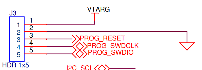
So what does that mean to this design? Can the programmer run at 5V? There is a VTARG pin on the programmer which I have not connected to before. Can this just be connected to +5V? Or will that damage the programmer?
USB to the Rescue?
An ap note offers one tantalizing clue to programming the PSoC (Document #: 001-81290 Rev. *F).
PSoC 5LP has two pairs of pins that support SWD: P1[0] SWDIO and P1[1] SWDCK,
or P15[6] USB D+ (SWDIO)  and P15[7] USB D– (SWDCK) pins.
No device configuration setting is required to choose between these two pairs.
The internal device logic chooses between these pins automatically by detecting
activity (clock transition on SWDCK lines) after the device comes out of reset
Sounds like the USB could be used to program the PSoC. Well, my ODAS-PSOC5 board has a USB connector so I should be able to try this easily enough. Not now, though,
Another clue comes from the schematic for the Programmer.
The USB connector on the programmer connects through a protection diode to the target. That means that the target can be powered from the programmer and (more importantly for this application) the programming interface can be run at 5V. In fact, it also explains why I had problems when I connected the target voltage to a target which was powered at 3.3V. The diode would have been forward conducting. It's a good thing they have that PTC fuse to protect the programmer or I might have blown the programmer and the host USB port. Moreover, the schematic for the programmer shows VTARG connects directly to the programmer header pin.
Pick One or the Other - How about both?
Not sure which method (USB or SWD connector) is best to use so I will leave both options. At the very least I know the SWD header interface works for programming. And I now know it can be operated at 5V.
Measuring the voltage on my PSOC card shows it's at 4V nominal anyway. And VTARG is at 5V so this seems like the way to go. It looks like it should be safe to connect all four I/O voltages directly to 5V.
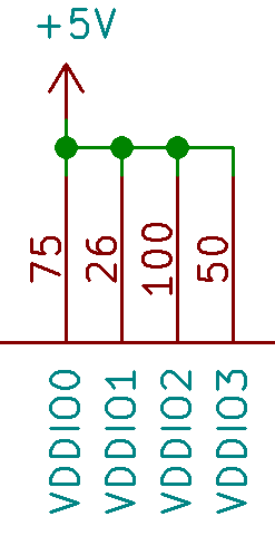
PSoC Power
The PSoC power system seems complicated at first blush. But the PSoC can be powered from VDD=5V which pretty much sets it in its own class. There are internal regulators for the core, etc. The reference from the datasheet shows the connections:
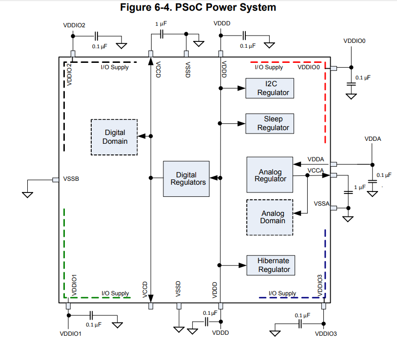
It is important to not connect to VCCA and VCCD. They need capacitors to ground but other than that get left unconnected. The two VDDD connections are made internally so they don't have to be connected externally. Just add caps on each pin. Connecting the VDDA to VDDD should be OK but I'm going to have a spot for a chip inductor to reduce noise on the pin.
There also needs to be a bunch of 0.1uF bypass caps near the pins of the PSoC and one by each of Z80 parts.
Clocking the Card
We need the following clocks.
- PSoC clock - Up to 67 MHz
- CPU clock - Up to 6.17 MHz supported by the speed grade of Z80 that we have
- Baud Rate clock - Support for 115,200 baud
- Optional 32.768 KHz for the real time clock
Clock Source
The card came with a 4.9152 MHz can oscillator which can be used as the clock source into the PSoC.
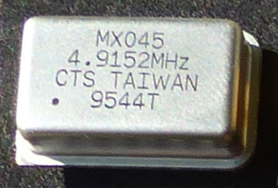
The MXO45 is made by CTS and it a 5V part. The data sheet shows:
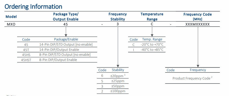
The part only has the 45 with no dash numbers, etc so we really don't know too much about the part. We do know that no output enable is required (we need to know that for the schematic). We can probably assume that it's the lowest accuracy grade which is 100 ppm which is 0.01% accurate. Not a bad choice for clock. And I've already got the part.
PLL Resources on the PSoC
The external oscillator can be used to create the other clocks via the PLL in the PSoC. The ap note AN60631 - PSoC® 3 and PSoC 5LP Clocking Resources describes the PSoC clock circuitry. Here's the basic block diagram:
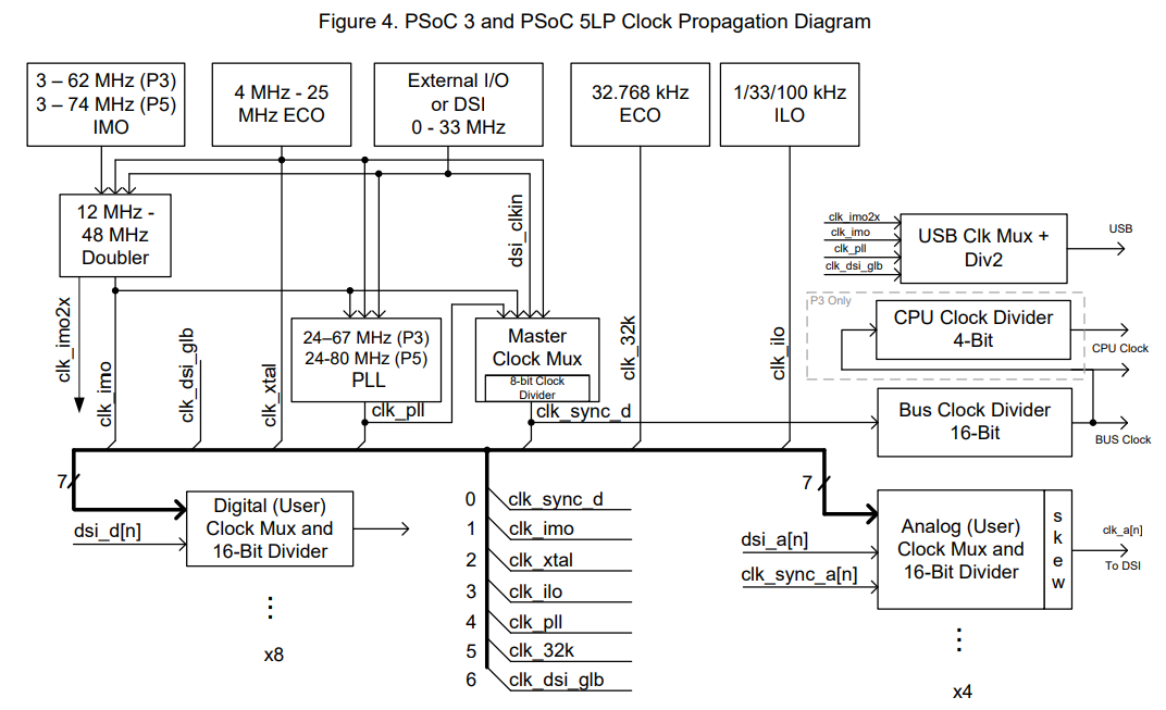
PSoC Clocking
The maximum clock rate of the PSoC is 67 MHz. Dividing 67 by 4.9152 is 13.63. The PSoC can multiply by 27 and then divide by 2 to get a multiple of 13.5. That means that the PSoC can be run at 66.3552 Mhz which is close enough to the 67 MHz maximum.
CPU Clock
The data sheet says that the Z80's 6 MHz clock can be clocked at 6.17 MHz. If the PSoC is running at 66.3552 MHz then dividing this clock by 11 would be a clock at 6.032 MHz which is as close as possible to the maximum 6.17 MHz using integers.
If the clock is 66.355 divided by 11 (5/6 clocks may be symmetric "enough") that would result in a 6.032 MHz clock to the Z80. Not quite the 6.17 MHz that that data sheet indicates the part can run but certainly much better than the 4.9152 MHz that the oscillator produced.
The CPU clock doesn't have to be symmetric as long as it doesn't violate the clock pulse width low/high widths. These times are 65 nS for the Z80.
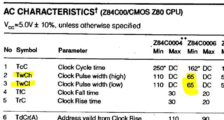
Since the 6.032 MHz clock is the 66.353 MHz clock divided by 11, the clock ends up having a 5/6 clock duty cycle of the 66.353 MHz clock. That's 75 nS/90 nS which is more than the spec 65 nS. So that looks good.
Baud Rate Clock
The baud rate clock rate for 115,200 baud is 16x the 115,200 baud or 1.8432 MHz. Dividing the 66.3552 Mhz by 1.8432 MHz is a clock divisor of exactly 36. Works out really nice.
Real Time Clock Oscillator
This is a cheap watch crystal at 32.768 KHz.
Clock Choice
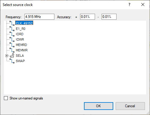
So, it looks like using the crystal oscillator that came with the parts should be useful. Let's take a look at how to drive the PSoC from an external clock source (the kind that comes in a can not a crystal). In the PSoC the clock can be driven externally into a Digital Input pin. First, we need to add an input pin to the schematic and name the signal so we can tell the clocks page which signal to use (it has to use an already existing signal). This is created as the previous pins.
Next we need to tell PSoC Creator we want to use the signal as an external clock. Go to the Configure System Clocks screen and turn off the XTAL by deselecting the check box. Then, click the check box in the Digital Signal box and select the signal we just made (the [...] button gets you there). This will initially produce an error because PSoC Creator doesn't know the characteristics of the clock.
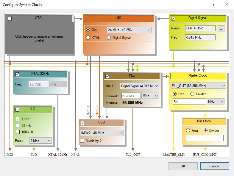
Next, tell PSoC Creator that the external frequency is 4.9152 MHz. We could set the accuracy if we wish, but don't need to. Select the signal using the [...] button and set up the values. We can set the accuracy of the oscillator to the presumed 0.01% determined earlier from the part data sheet (worst case part).
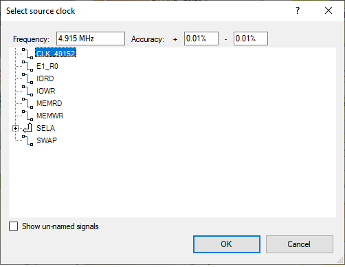
We had to set up the IMO to be 24 MHz and the USB [clock] to be IMOx2. The IMO is internally trimmed to 24 MHz +/- 0.25% so it's plenty enough accurate for the USB (it was recommended by the clock planner). In fact, the IMO is the root of some of the issues here since there's no accurate way between the IMO frequency and the PLL integer values to get the precision we need for a baud rate. Hence the external crystal.
This configuration produces no errors so it should be legal. Here's the final result:
Final Clock Solution
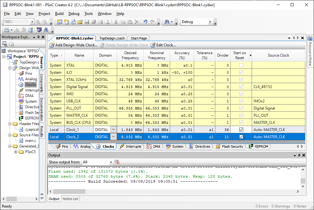
Summary of Clocks
- A 4.9152 MHz oscillator came with the other parts
- Add the 4.1952 MHz crystal to the schematic on a digital input pin into the PSoC
- The 4.9152 is multiplied up by 13.5 by the PLL in the part to produce a system clock of 66.353 MHz which is just short of the 67 MHz maximum clock rate of the PSoC
- The CPU clock is 66.353 divided by 11, or 6.03 MHz (Close enough to the 6.17 MHz possible with the part)
- The baud rate clock is 66.353 divided by 36 or 1.8432 MHz which gives a 16x clock for 115,200 baud. This is accurate to 0.01% (essentially the external oscillator accuracy).
- The first XTAL is not used.
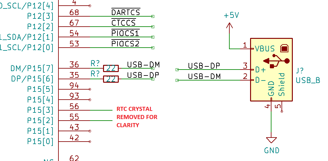
Chip Selects
The next challenge is figuring out which control lines must go through the discrete logic and which can connect directly between the other parts. Certainly, all of the chip selects have to come out of the PSoC. These are:
- EECS* - EEPROM Chip Select
- SRAMCS0*, SRAMCS1* - SRAM Chip Selects
- DARTCS* - Dual UART Chip Select
- CTCCS* - Counter/Timer Chip Select
- PIOCS1*, PIOCS2* - Parallel I/O Chip Selects
Some, but perhaps not all, of the control signals to/from the Z80 need to come into and possibly out of the PSoC. These are:
- CPUCLK - Clocks the CPU and other logic that uses the CPU's clock
- RESET* - Resets the CPU under control from the PSoC
- RD*, WR* - Read and write signals from the Z80
- IORQ* - I/O Request
- MREQ* - Memory Request
- BUSRQ* - Bus Request can be used to request the bus for programming the EEPROM
- BUSACK* - Bus release acknowledgement - tells us that the Z80 has released the bus
- WAIT*, HALT* - Could be useful - perhaps for single stepping?
UART lines
We should hook up enough lines for a full duplex UART connection. Having flow control is really helpful for downloading to slower CPUs. The lines are:
- SER_P2D (Serial, PSoC to DUART)
- SER_D2P (Serial, DUART to PSoC)
- RTS
- CTS
- UART Clock
I like the SPI naming convention which includes source/destination and makes it easier to keep track of which pins are in/out.
Other lines?
Should we hook up lines from the counter/timer?
Address/Data Bus Lines
There's plenty of I/O on the part to connect all of the 16 address and 8 data bits. That way we can fully decode the addresses and read/write data from//to the PSoC. These pins can also needed to program the EEPROM on the board.
Memory Banks
If we want to have memory banks (we only have 64K of SRAM so this isn't too useful) we need to control some of the upper memory address bits. At the very least we need to have a control register inside the PSoC that we can use to swap the EEPROM out and run from SRAM.
It could also be useful to have different EEPROM sizes. We are using a 64KB part and if we control the upper address bits we could scale the memory size up/down without using any jumpers on the board.
These are sufficient reason to control at least the upper few address bits. At power up the memory map could be pre-configured to come up with a specific configuration based on how much EEPROM space is used by the program.
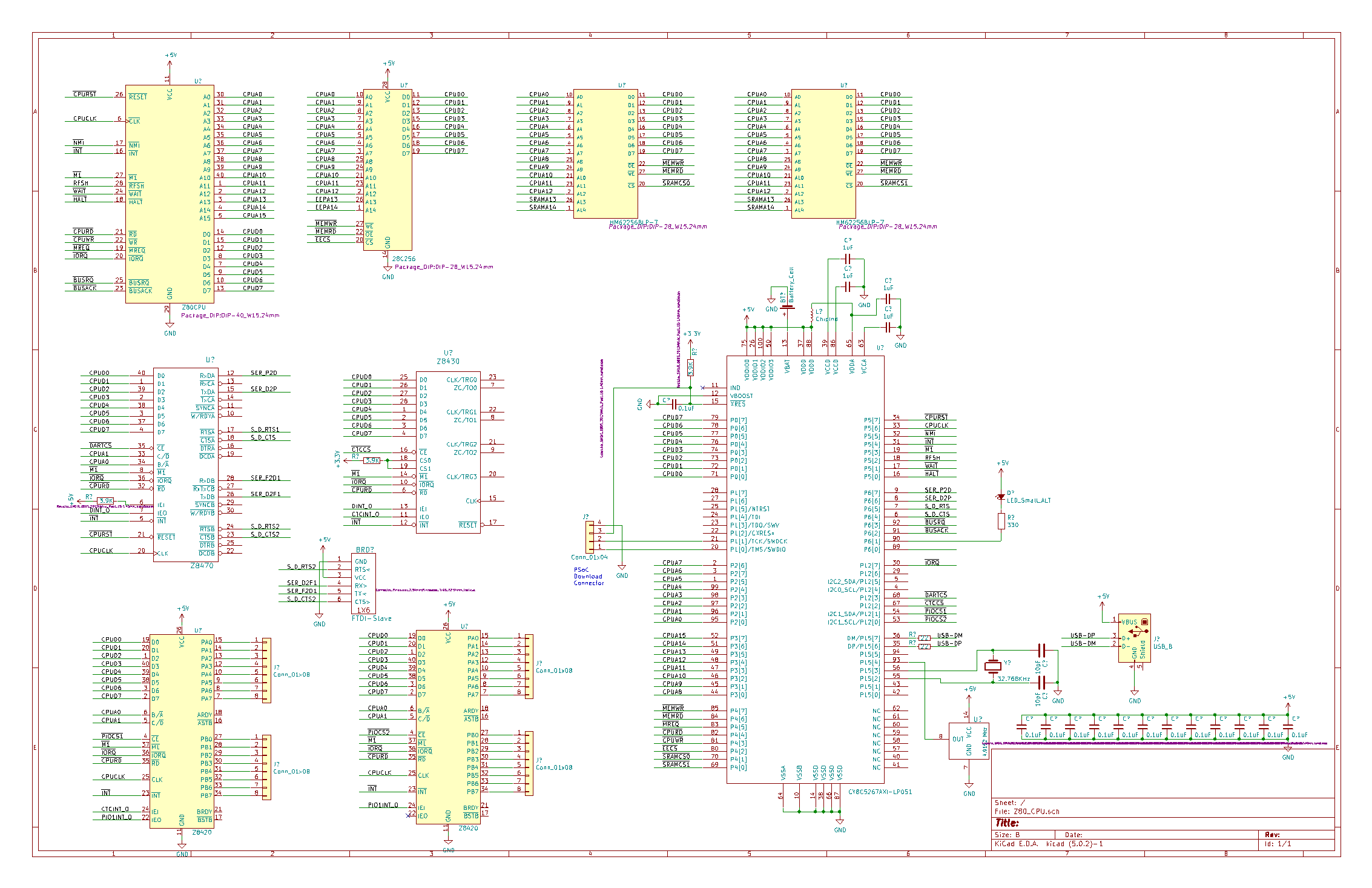
Schematic
So far, the schematic now looks like:
BOM Cost vs Discrete Solution
Used the Zeta SBC V2 for comparison. All of these parts are contained within the PSoC.
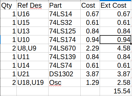
That's not including the USB-to-Serial. Turns out the BOM cost is about half of the discrete solution. Add to that the savings in board space and the PSoC comes out on top.
First Example Z80 Configuration
I'm going to implement Grant Searle's 9-chip Z80 design in the PSoC and see how it fits. Should be easy enough. Grant's SIO chips run at 7.3728 MHz which is 4x the 1.8432 MHz so the PSoC synthesizer has no issues with that. His schematic does remind me I need to hook up the UART clock lines to the PSoC. My chipset is 6 MHz so this won't be what I will use. I just want to see how easy it is to make other configurations.
U7A, U7B are the crystal oscillator and are in the PSoC.
Grant has two pushbuttons for Cold/Warm reset. The Warm reset doesn't reset the peripherals like the cold reset does. I'll add a pin for warm reset to the PSoC but if I run out of I/O pins it will be the first thing to go.
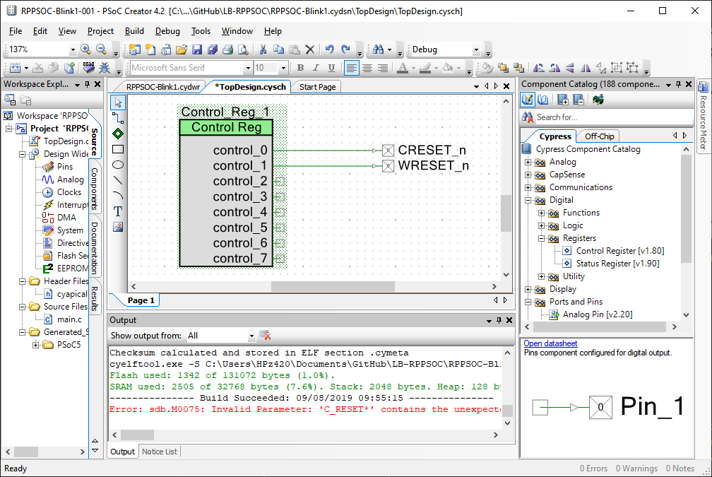
I'll put these two bits into the PSoC as a control register. The register will initialize to zero so the Z80 will be reset at boot until the PSoC turn it on. That looks like this:
Grant's I/O decoder is minimal. He has three chip selects:
- SIO @ 0x00-0x07
- A0 goes into B/A*
- A1 goes into C/D*
- This seems logical and probably can be hard-wired for most examples (need to verify others do the same thing)
- IO Chip Select @ 0x10-0x17 - Grant brings this to a header
- Bank Switch @ 0x38-0x3F - ROM is selected at cold start and when this address is written the ROM is switched out for SRAM
This decoder is relatively simple. Rather than doing AND-OR-NOT gates I'll just let the compiler reduce the logic. Here's what it looks like:
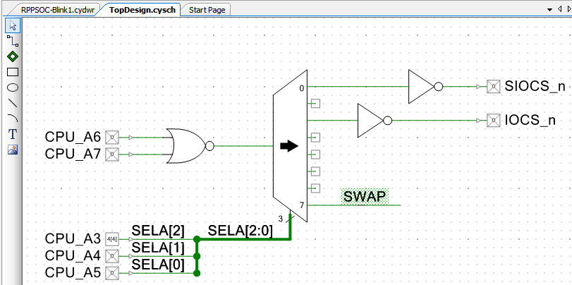
If A6 and A7 are both 0's then the output of the NOR gate is 1 and the 3:8 decoder will drive an active high output on the address decoded from A3..A5. The two chip selects are brought to an output pin and the SWAP line when activated will cause a switch between RAM and ROM.
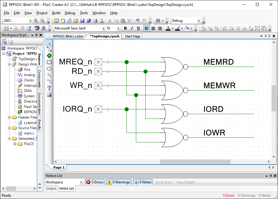
Grant also has logic to generate IOWR*, IORD*, MEMWR* and MEMRD* strobes. These are used to qualify chips selects and strobes. These can be made active high by using NOR gates instead of OR gates.
The SWAP of RAM and EPROM chip selects happens when an IOWR is done to the correct IO address. Grant does this with a cross-coupled latch (Set-Reset) latch. This can be done in the PSoC with an RS-Flip flop. The RS-FF can be synchronous, too. It gets cleared by Cold Reset and set by the write. Here's the circuit:
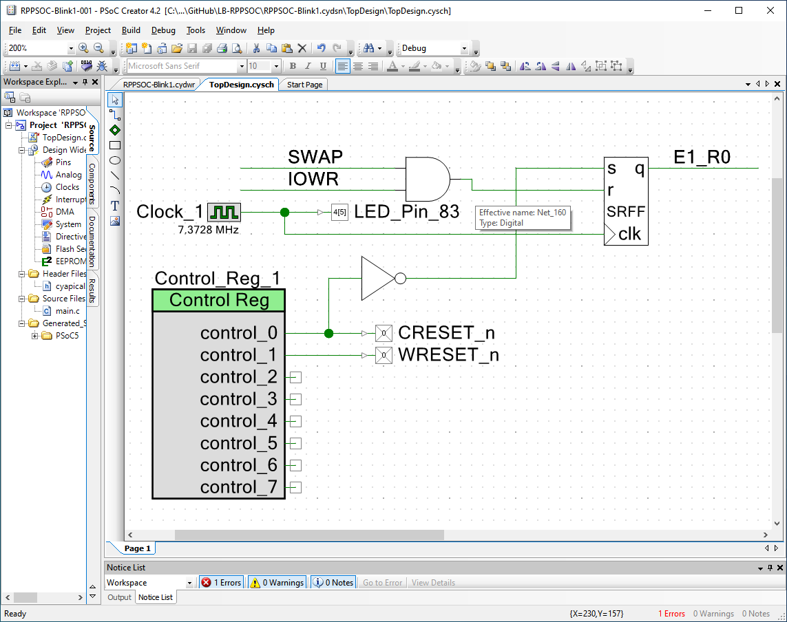
The completed chip select logic is:
I'm away from my personal PC with PSoC Creator at the moment so this will be just a sketch of changes I'm going to make.
I/O Address Decoders
For the I/O address decoders, I'm considering replacing them with comparators. One input would take the address lines 0-7 bottom address bits (depending on the peripheral chip - some use 1 or 2 bits for register selection). The other input of the comparator could be either a constant or even a register loaded by the ARM CPU. This will make a very flexible I/O space which could be re-targeted without changing the logic for each design.
There are 4 chip selects which need to be created.
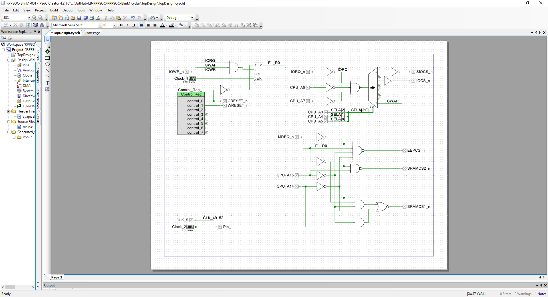
- CTCCS*
- DARTCS*
- PIOCS1*, PIOCS2*
The CTC chip select will compare all 8 address bits (a0..a7).
The DART uses 2 address bits so the chip select will compare 6 address bits (a2..a7).
The PIO chips use 2 address bits so the chip select will compare 6 address bits (a2..a7).
This should be the most flexible approach and will be completely programmable from the PSoC. That means different firmwares should be able to be run without recompiling the FPGA.
Do I Need EEPROM?
I'm going to put a 28C256 EPROM onto the card, but the question is whether I need this or not. The program could be downloaded directly into the RAM and the CPU released from reset. But that would not allow existing software which does this copy to run without source code changes.
So, I'm going to put a big EEPROM with the ability to select different sizes/builds.
Test Layout
I did a quick layout of the PCB to see how big it is and how much it would cost.
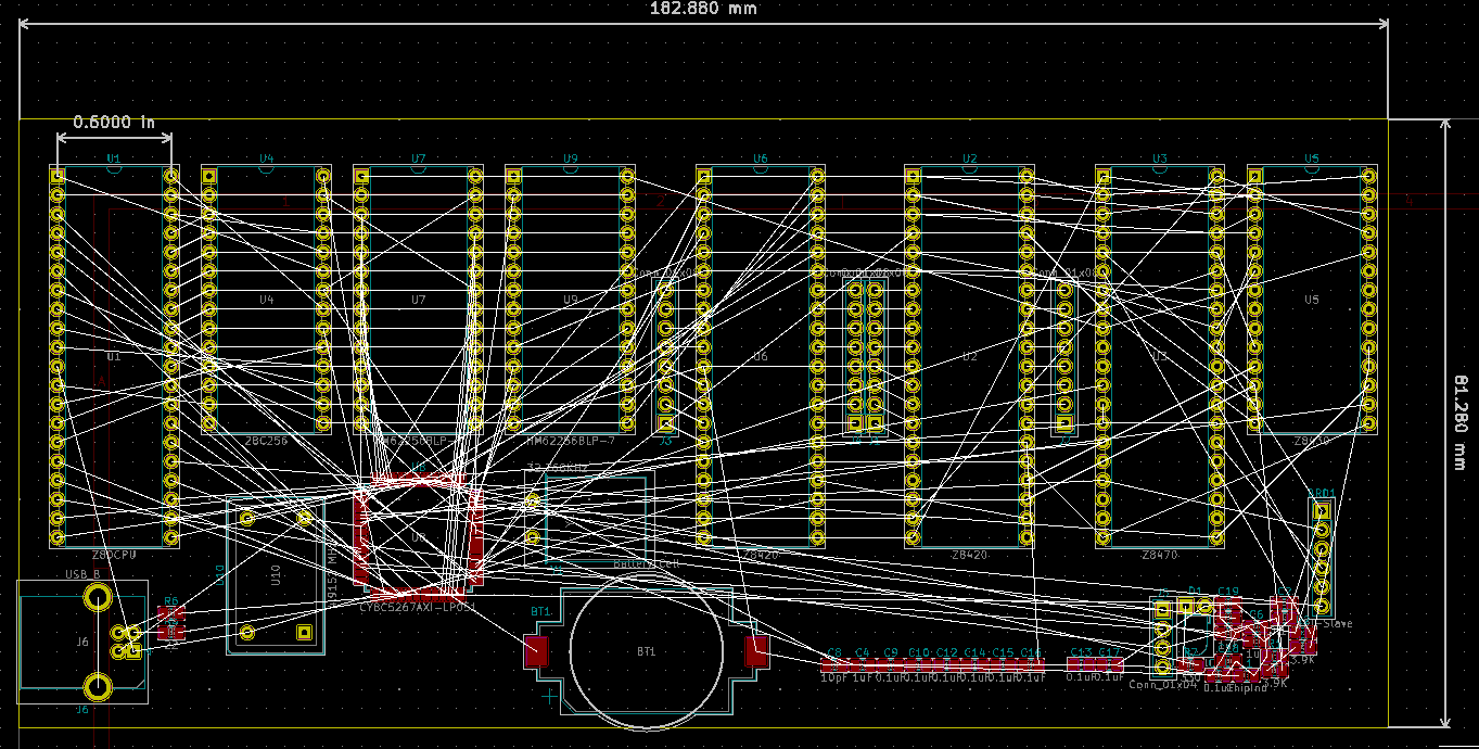
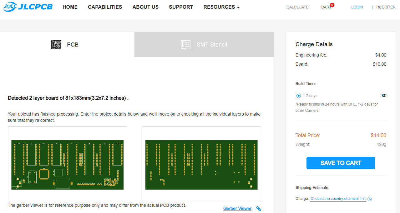
With everything side by side it's over 180 mm by 80 mm. JLCPCB gives a quote easily for qty 10 boards ($14 plus shipping). Not too bad.
This is reasonably close to the 100x160mm size of the ECB. However, my goal is to use all of the Zilog chips and putting them in a row makes for a much easier layout.
A Completely Different Possible Approach
Leaving only the Z80 and adding a higher density SRAM could result in a 3-chip solution. Use the Z80, PSoC and a high density SRAM along with the oscillator. All of the I/O could be performed in the PSoC.
A three chip Z80 design schematic would be something like:
This has a 512KB SRAM, the Z80 and the PSoC. The oscillator wouldn't be needed unless precise serial connections were needed.
The PSoC could easily emulate the control/status registers of the DART/SIO and CTC. Parallel I/O could be easily added with an optional MCP23017 chip which would only need to connect to I2C pins on the PSoC.
This is very similar to the Z80-MBC2 board without requiring the complications of the ATMEGA interface. In that design, the ATMEGA interfaces to the CPU force feeding it instructions with boot stages.
In this design, the PSoC downloads the software to the SRAM and takes the Z80 out of reset. Also, hardware/software implementations which have both EPROM and RAM could be "emulated" by banking the SRAM. Control of upper RAM address bits allows a bank of the SRAM to work as an EEPROM. The program can be downloaded from the emulated SRAM into the SRAM itself.
The Z80 peripherals can be emulated. For instance, the DART/SIO would consist of data and control/status registers which are I/O mapped to the Z80 and memory mapped to the PSoC.
Counter/Timers could also easily be simulated in PSoC hardware.
The PCB would be cheaper since it could easily be built in a board that is smaller (less than 100x100mm which is the sweet spot for PCB designs.
I am going to make a project page for this concept.