 land-boards.com
Loading the initial SRAM contents falls out of the previous design considerations with a couple of minor additions to control logic.
SRAM address lines A0-A7 are handled as follows:
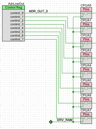
An 8-bit control register contains address bits 0..7. The next section of logic creates address bits 8..10 and the DRV_RAM signal which drives the address lines onto the address bus of the Z80. The Z80 must have surrendered the bus via either:
- Being held in reset by the PSoC
- Bus surrendered by the PSoC asserting BREQ* (Bus Request( and granted by the Z80 asserting BGR* (Bus Grant).
The first method is the most obvious since the CPU won't run until a program is loaded into it.
Address lines 8..10 are controlled as follows:
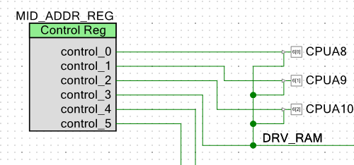
These mid range addresses as well as the DRV_RAM control signals are all output from the PSoC MID_ADDR_REG register.
The upper address lines fall out of the memory mapper described in the previous log post.
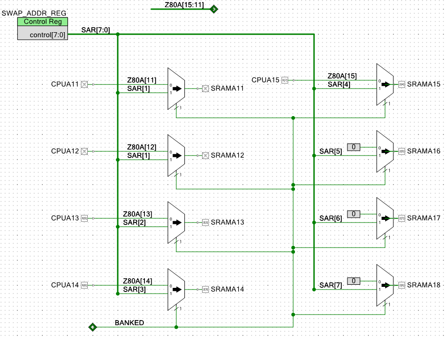
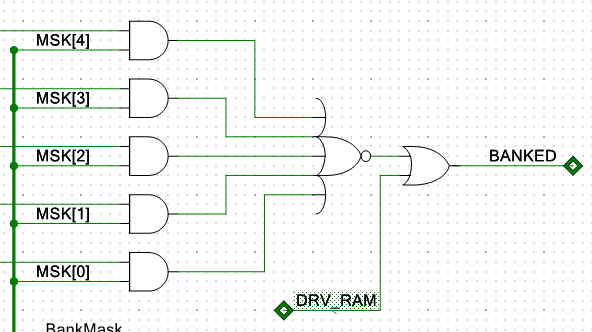
The SRAMA11..18 lines are the value of the SWAP_ADDR_REG. They don't need to be trisstated since they only go to the SRAM. There needs to be an additional factor in the BANKED signal, namely the DRV_ADR which should force the multiplexers to always use the SWAP_ADDR_REG as the source of address during loads of SRAM. DRV_ADR is added to the comparator output as follows:
Control Logic
The control logic for loading SRAM is conventional and fairly uncomplicated. It is contained in the same register that controls the mid addresses (above). It looks like:
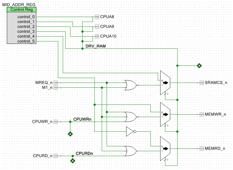
There are 2 output bits. One is Read/Write which controls the MEMWR* and MEMRD* and the other strobes the SRAMCS*.
Data Bus
There is a register (the Z80_Data_In register) which puts data out on the Z80 data bus. It's already used for I/O reads from the Z80. This same register can be used to put data into the SRAM.
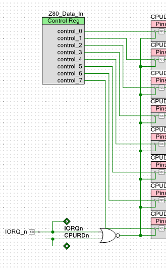
The control signals need to include the DRV_RAM signal and the MEMWR* control lines. Here's that added logic:
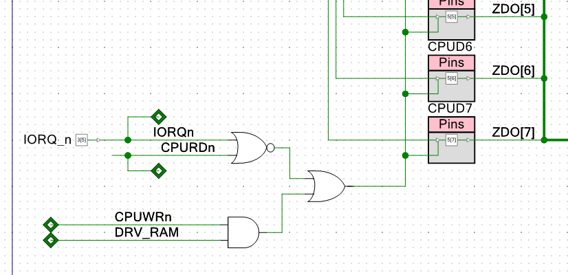
That should be all that is required to load the program into the SRAM.
Discussions
Become a Hackaday.io Member
Create an account to leave a comment. Already have an account? Log In.