 land-boards.com
Made some changes to the address mapper/bank switch hardware to support Grant's bank switching.
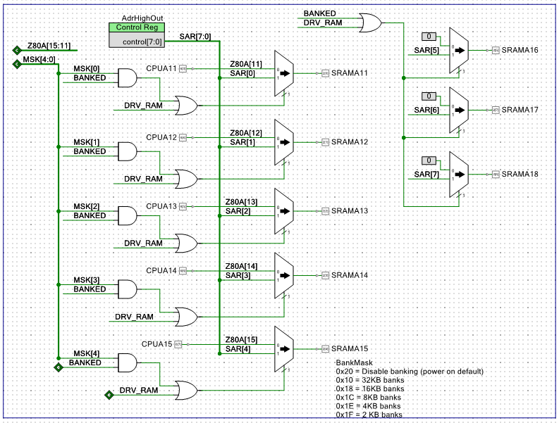
Signals are:
- DRV_RAM - asserted when the PSoC was testing the SRAM at power up and when Z80 code is loaded into the SRAM to be run.
- MSK[4..0] determines whether the address is used when the bank SRAM is accessed.
- Z80A[15..11] is the address directly from the Z80.
- BankMask MSK[]4..0] is the number of bits that are replaced is determined by this.
- SRAMA[18..A16] are all zero's when the access is to spaces other than the bank.
- SRAMA[18..16] are set from the SAR[7..5] when the BANK is selected.
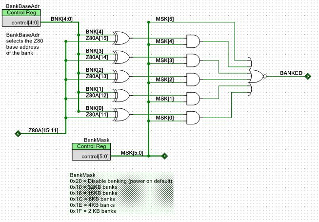
Set the Base Address for comparison to the first 8KB of SRAM which asserts the BANKED line.
Needed to add in the MSK bits into each individual address select mux. The BankMask is set to 0x1C for 8KB banks. That means that the Z80A11 and A10 bits are passed through directly and only when the address is in the range of the first 8KB is the selection from the AdrHighOut.
The Bank Base Address comparison logic looks like this.
With the previous logic the board rebooted when I did a cold boot.
After making these changes the board booted correctly. The Bank logic initialization code looks like this:
#define BANK_SIZE_32K   0x10
#define BANK_SIZE_16K   0x18
#define BANK_SIZE_8K    0x1c
#define BANK_SIZE_4K    0x1E
#define BANK_SIZE_2K    0x1F

// Memory Mapper version 1 sets bank size to 8KB
// Points to the first SRAM bank

void init_mem_map_1(void)
{
    BankBaseAdr_Write(0x00);
    BankMask_Write(BANK_SIZE_8K);
    AdrHighOut_Write(0x00);
}
This logic is pretty general purpose and could support multiple pages if the Z80 wrote to a bank select I/O address. Grant's code only goes a single swap of the spaces.
Grant's code only switches out the 8KB bank for another bank. This function does the switch:
/////////////////////////////////////////////////////////////////////////////////
// void swap_out_ROM_space(void) - When called switches to the 2nd bank
// Used with Memory Map 1 scheme where there's a single 8KB bank starting at 0x0000
// which is switched out when an I/O location is written.

void swap_out_ROM_space(void)
{
    AdrHighOut_Write(0x20);     // Set A18..A16 to 0x1
    ackIO();
}
Other memory maps would need their own functions, so I've bracketed the code with a #define to indicate it only applies to this software build.
The weakness of this scheme is that it really doesn't take good advantage of the extra memory. After all, we've got 512KB and are only using 64K + 16K = 80K of the 512KB. But for CP/M this is probably just fine.
Not an MMU
This isn't really quite an Memory Management Unit (MMU) since it would need to be able to swap multiple spaces rather than just one space. An MMU would take additional comparison logic as well as muxes to select the right addresses. Optimally this could be done with a fast RAM which would associate addresses from the Z80 to bank addresses on the output which would get routed to the SRAM as the upper address bits. The PSoC isn't optimal for this since the logic in the part is limited. But a few bank selects could be created which are basically just copies of the above logic plus additional multiplexer inputs.
One use of such a scheme would be to support a RAM disk. After all, the 512KB could be put to good use if it were made available. But this would take a bit of support from the CP/M code itself.
Grant has a 128KB version of CP/M which could be promising for this approach. May investigate later one.
Discussions
Become a Hackaday.io Member
Create an account to leave a comment. Already have an account? Log In.