 Ken Yap
A DTL binary clock
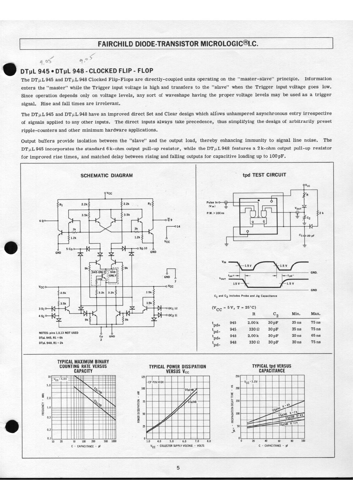
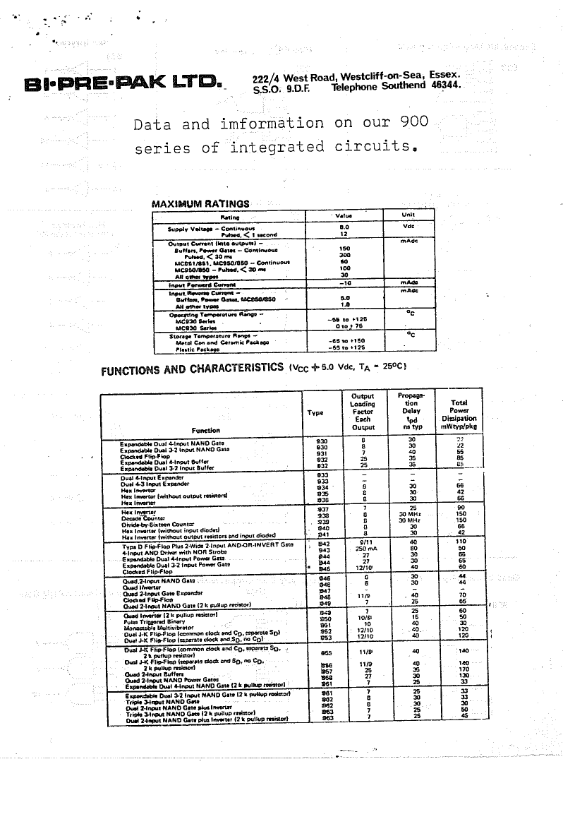
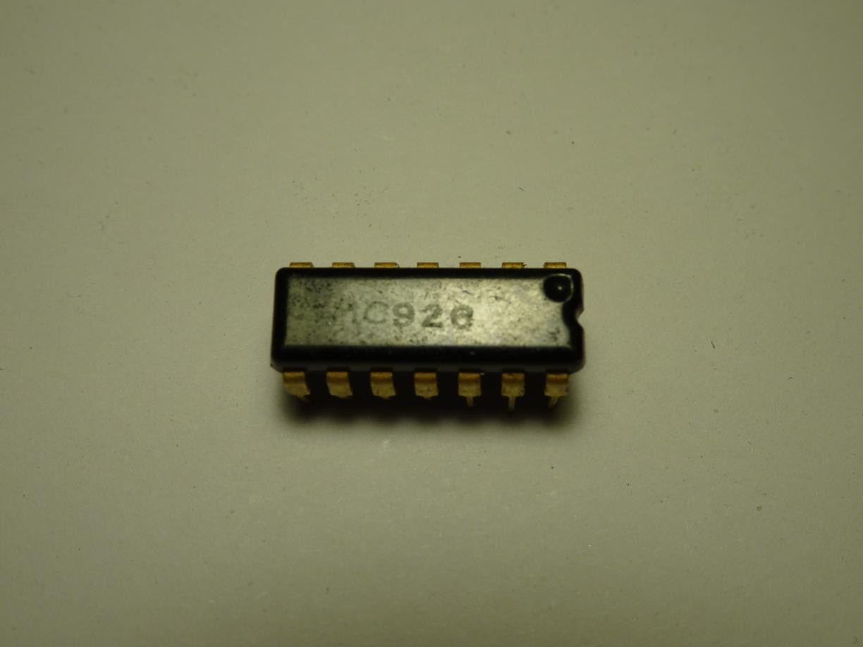
I found that I have a dozen DTµL945 master-slave flip-flops from about 50 years ago in my retro collection. These Diode Transistor Logic (DTL) chips are truly small scale integration. Even TTL packed 4 or 8 flip-flops to a package. What to do with them? Here is the data sheet for it.
Overview
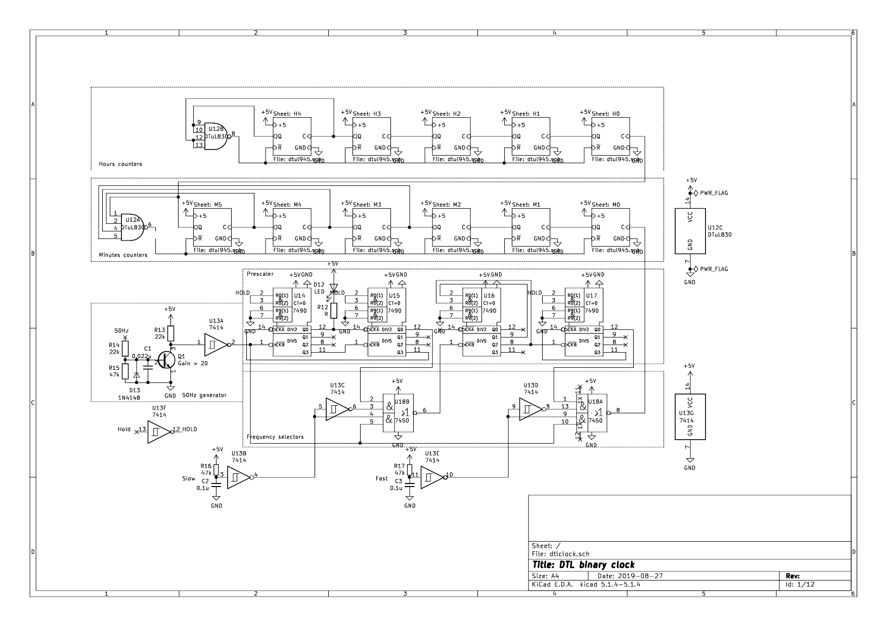
The only viable project I could think of was a binary clock. I can't even do BCD hours and minutes, that requires more chips than I have. I can only do sexagesimal hours and minutes. 0-23 requires 5 bits, and 0-59 requires 6 bits. I also need a 2-input NAND gate to reset the hours at 24 and a 4-input NAND gate to reset the minutes at 60. I have the DTµL830 which has dual 4 input NAND gates. This has the same pinout as the TTL 7420, and in fact I used the library symbol for that. The LEDs are driven directly from the flip-flops.
Designing with DTL is very similar to designing with classic TTL, after all TTL was a development from DTL. The main difference is that there is no active pull up on DTL outputs so rising edges are not as sharp, limiting the speed. For this clock the highest frequency in the circuit is 50 Hz so this is of no consequence.
Now the components of the design, starting from the frequency input. Here is the circuit I designed in the first round of this project with blocks indicated. See below for the newer version.
Time reference
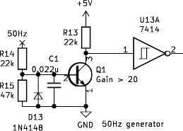
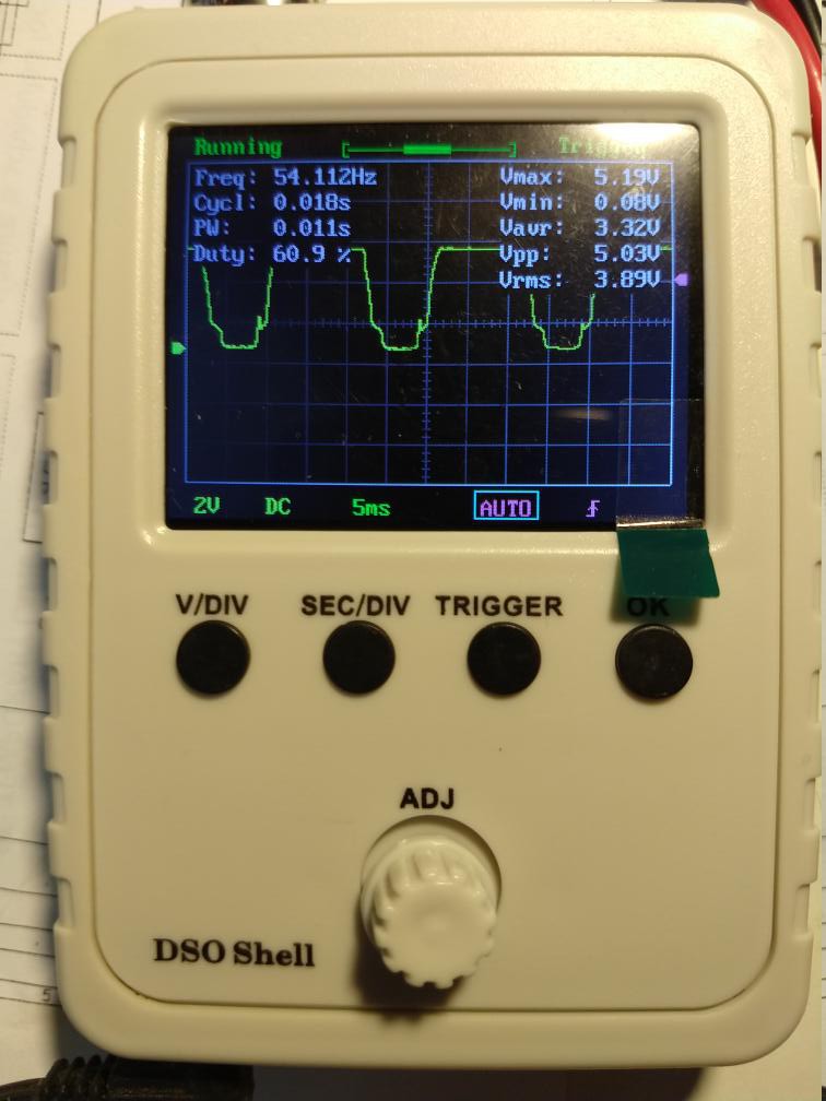
I decided on 50 Hz mains so I have to prescale the input by 3000. I can do this with 4 TTL 7490 counters of which I have a lot. This means the design is not pure DTL but still retro. By adding a TTL 7450 dual AND-OR-INVERT gates as two-input selectors I can bypass part of the chain so that the hours and minutes can be set quickly. A TTL 7414 hex schmitt trigger for debouncing the switches and providing the inversion for the 7450 gates completes the line-up. One discrete transistor squares the sine wave from the transformer. For power I have to use an old-school step-down transformer, rectifier, and a 7805 voltage regulator chain, as a SMPS won't provide the 50 Hz reference. These power wall warts are getting rare. If I'll be making more mains frequency driven clocks I may have to put out a call to a local recycling group to snarf all the old power transformers left. 😀
Prescaler
The 7490 has separate divide by 5 and divide by 2 sections, so they can be used in two configurations. The first two 7490s divide by 5 twice then divide by 2 twice. This gets us a square wave rather than a 20% duty cycle wave. This is useful so that the pilot LED has a symmetric blink. If a calmer blink of 0.5 Hz instead of 1 Hz is desired, the LED can be driven from the divide by 2 output of U15 instead of U14. The penultimate 7490, U16, divides by 3, with outputs for 2^1 and 2^0 ANDed to reset to 0 after 2. The last stage U17 divides by 10 (5*2) and the output is a 1/60 Hz square wave, i.e. period of one minute.
Binary ripple counters
The master-slave DTµL flip flops feed the Q and Q' outputs back to the inputs crossed so that each clock pulse will invert the state, thus dividing by 2. The wiring looks hairy but each stage is wired identically. For the minutes the 32, 16, 8 and 4 flip flops go to a NAND gate to reset at 60. For the hours, the 16 and 8 flip flops go to a NAND gate to reset at 24.
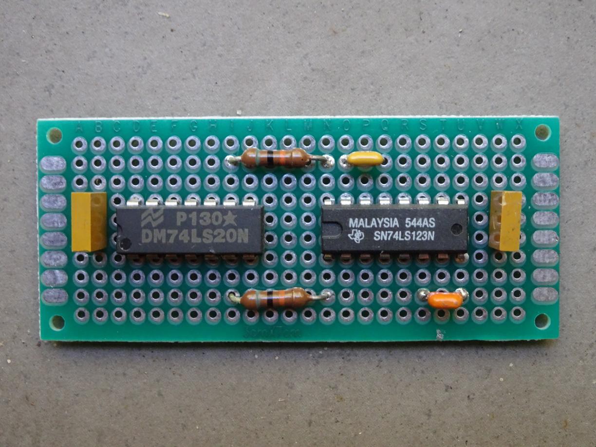
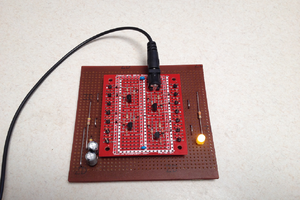
I used sockets for the DTL chips in case I need to replace counters or gates. Or rather one counter I have only one spare. 😀
LEDs
The Q' outputs of the binary counters sink current so when Q' is 0 the LED lights up, i.e. when Q is 1. TTL/DTL outputs can sink much more current than they can source. One unit load is 1.6 mA. Most gates drive 10 ULs so up to 16 mA can be sunk.
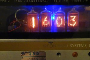
I used greenred LEDs for the hours and redyellow LEDs for the minutes to make it easier to read. I also used rectangularsmaller LEDs for the high nybble. The pilot 1 Hz LED at the bottom uses an ambera blue LED. It also helps to orient the viewer when many LEDs are off.


 agp.cooper
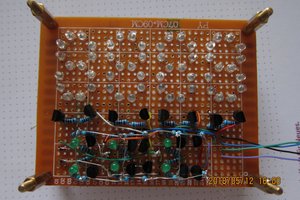
 Pavel
Pavel
 Dave Gönner
Oh ! How did I miss this project ?
I'm a discrete clock wannabe DIYer and want to play with the various types of logic so any and all details are welcome !