 Ced
CedCPUs are mainly temporary storage stuff with routing capabilites. To perform operations on data there is first the need to locally store this data (coming from memory, ROM or IOs) within the CPU.
There are even many types of registers in a CPU:
- general purpose registers (used to manipulate data)
- intruction registers (storing the instruction that is going to be executed)
- program counter (a special kind of counting register used to store at which step the program is currently positionned)
- address registers (pointers to memory)
- stack registers (also a pointer to memory but used for specific stack instructions)
- I/O registers used to communicate with external devices
- etc
Registers can vary in width depending on the CPU (from 8 bits to 128 bits). In our example they will all be 8-bit wide as we only have 8-bit data and 8-bit address capability.
In the following we only talk about the general purpose registers (couting registers will be discussed later).
So what are the functions of a general purpose register in the context of our CPU:
- load information from the bus when instructed to
- store the information until an action is performed or power is turned off
- display the information using LEDs
- 'publish' the stored information onto the bus when instructed to
- reset the information (or clear). This means putting all the bits to 0.
Therefore we can see there is the need for 3 signals to instruct the register what to do:
- register_in : load the information from the bus
- register_out : publish the information to the bus
- register_clear : clear the content of the register
However, something is key for a register : it's the timing of the loading function. Its has to be performed in a snapshot. This is why registers input the value from the bus on the rising edge of the clock. Therefore there is the need for 2 signals when inputing the values from the bus:
- the action signal register_in : the signal that informs the registers that it is going to load and store the information available at its input (usually the bus)
- the clock signal of wich we only use the rising edge to define the precise moment at witch the information is taken from the bus
There are many ICs in the 74xx series that provide some of these features (so many choices).
In Ben's videos, he uses the 74LS173 (4 bit register with output enable signal, input enable signal, clock and master reset signal)
[Update : See my later post on register IC]
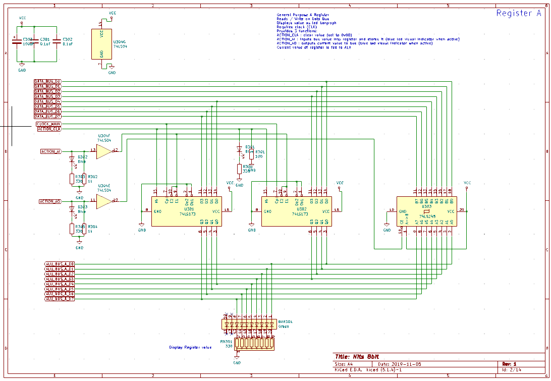
In practice we are not going to use the 3 state output and Output Enable capability of the 173 because we want to display the value of the register at all times on the LEDS. Therefore, the output is kept alway on. A separate chip is ised to provide the output buffering.
The 74HCT245 IC provides juste that : an octal buffer with 3 state output (it actually is bi-directional but we will use only one direction in this context). Note there is an existing single direction octal buffer, the 74HCT241 however the pinout is not as easy and in order to keep only one reference, we will use only the 245.
This chip offers 3 state output. This means that it can be seen as:
- output is activated and the value of the bit is 0 (0V)
- output is activated and the value of the bit is 1 (5V)
- output is deactivated and the chip is considered as not connected
So the outcome is that we need only 3 chips and a bunch of leds and resistors to implement a general purpose register.
Note that the diagram above shows 2 more elements not mentionned above : the link between the register and the ALU (out of topic for now) and some inverters on the action lines as the chips expect active low signals (this can be optimized later on, but for learning purposes it is better to show uniform active high action signals).
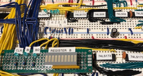
Preview of the prototype (using the original 74LS173 IC):
Discussions
Become a Hackaday.io Member
Create an account to leave a comment. Already have an account? Log In.