 hesam.moshiri
References
Article: https://www.pcbway.com/blog/technology/DC_to_DC_Buck_Converter_Adjustable__97__Efficient__3A.html
[1]: https://www.mouser.com/datasheet/2/277/MP2315_r1.01-478439.pdf
[2]: https://componentsearchengine.com/part.php?partID=930350
[3]: https://www.samacsys.com/altium-designer-library-instructions
A tiny DC to DC buck converter board is useful for many applications, especially if it could deliver currents up to 3A (2A continuously without heatsink). In this article, we will learn to build a small, efficient, and cheap buck converter circuit.
[1]: Circuit Analysis
Figure 1 shows the schematic diagram of the device. The main component is the MP2315 step-down buck converter.
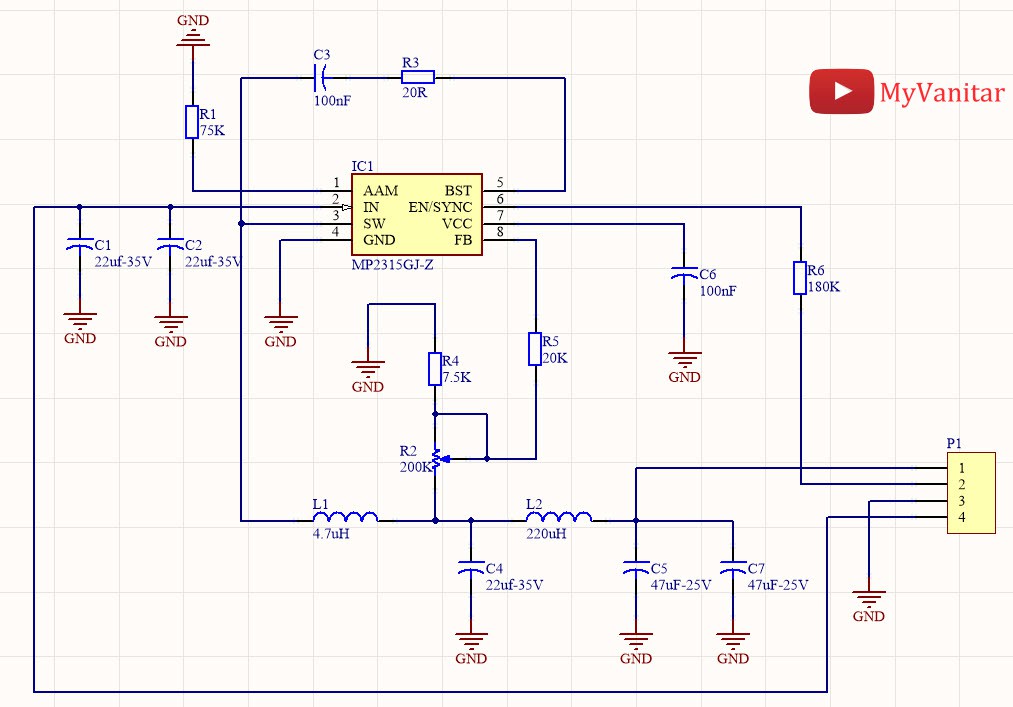
Figure 1, Schematic diagram of the DC to DC buck converter
According to the MP2315 [1] datasheet: “The MP2315 is a high frequency synchronous rectified step-down switch-mode converter with built-in internal power MOSFETs. It offers a very compact solution to achieve 3A continuous output current over a wide input supply range with excellent load and line regulation. The MP2315 has synchronous mode operation for higher efficiency over output current load range. Current mode operation provides a fast transient response and eases loop stabilization. Full protection features include OCP and thermal shut down.” Low RDS(on) allows this chip to handle high currents.
C1 and C2 are used to reduce input voltage noises. R2, R4, and R5 build a feedback path to the chip. R2 is a 200K multiturn potentiometer to adjust the output voltage. L1 and C4 are the essential buck converter elements. L2, C5, and C7 make an additional output LC filter that I added to reduce the noise and ripple. The cut-off frequency of this filter is around 1KHz. R6 limits the current flow to the EN pin. The R1 value has been set according to the datasheet. R3 and C3 are related to the bootstrap circuit and determined according to the datasheet.
Figure 2 shows the efficiency vs output current plot. The highest efficiency for almost all input voltages has been achieved at around 1A.
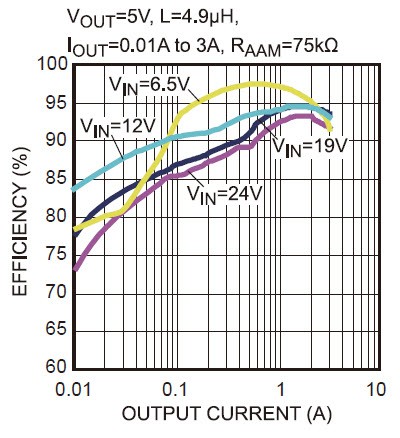
Figure 2, Efficiency vs output current
[2]: PCB Layout
Figure 3 shows the designed PCB layout. It’s a small (2.1cm*2.6cm) two layers board.
I used the SamacSys component libraries (Schematic symbol and PCB footprint) for the IC1 [2] because these libraries are free and more importantly, they follow the industrial IPC standards. I use the Altium Designer CAD software, so I used the SamacSys Altium plugin to directly install the components libraries [3]. Figure 4 shows the selected components. You can search and install/use the passive components libraries as well.
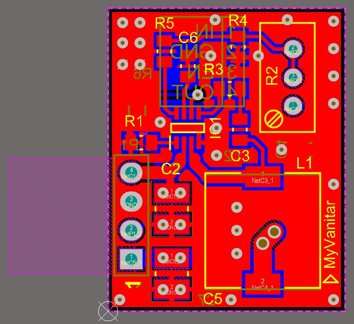
Figure 3, PCB layout of the DC to DC buck converter
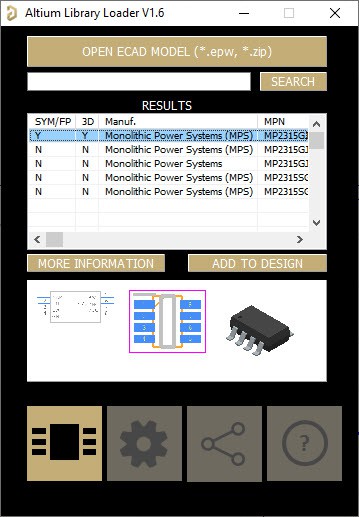
Figure 4, Selected component (IC1) from the SamacSys Altium plugin
This is the last revision of the PCB board. Figure 5 and figure 6 show 3D views of the PCB board, from the top and bottom.
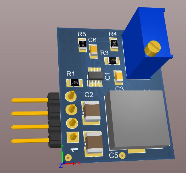
Figure 5, A 3D view of the PCB board (TOP)
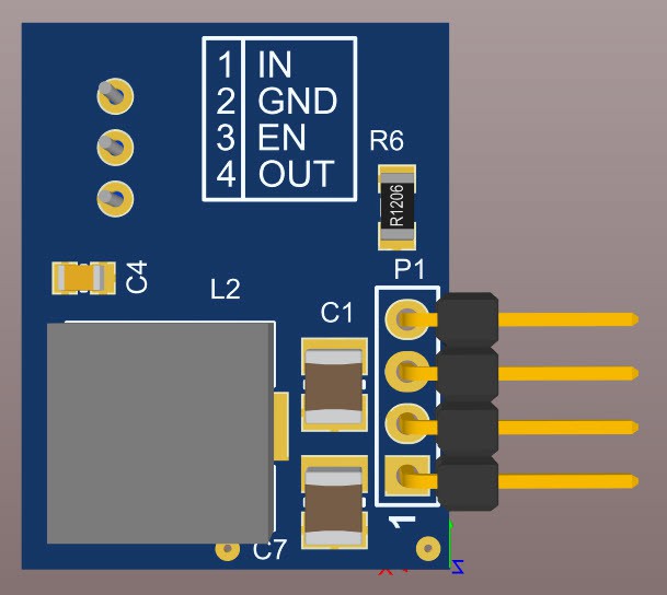
Figure 6, A 3D view of the PCB board (Bottom)
[3]: Construction and Test
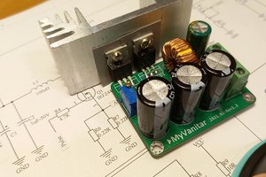
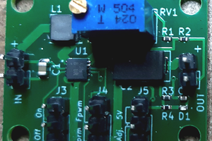
Figure 7 shows the first prototype (first version) of the board. The PCB board has been fabricated by the PCBWay, which is a high-quality board. I had no problem with soldering whatsoever.
As it is clear in figure 8, I have modified some parts of the circuit to achieve lower noise, so the provided Schematic and PCB are the latest versions.

Figure 7, The first prototype (an older version) of the buck converter
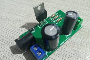
After soldering the components, we are ready to test the circuit. The datasheet says that we can apply a voltage from 4.5V to 24V to the input.
The main differences between the first prototype (my tested board) and the last PCB/Schematic are some modifications in the PCB design and component placement/values. For the first prototype, the output capacitor is only 22uF-35V. So I changed it with two 47uF SMD capacitors (C5 and C7, 1210 packages). I applied the same modifications for the input and replaced the input capacitor with two 35V rated capacitors. Also, I...
Read more »

 ElectronicABC
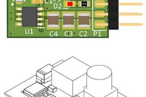
 Sergio Ghirardelli
Nice project. Have you measured the efficiency curves yourself to confirm it works as shown in the datasheet?