 Matthew James Bellafaire
It took awhile but we're finally here at the finished schematic of Revision 4. This log is really an electrical overview, of everything going on in this revision (since this is more of a re-design than a revision).
So lets start with the full schematic:
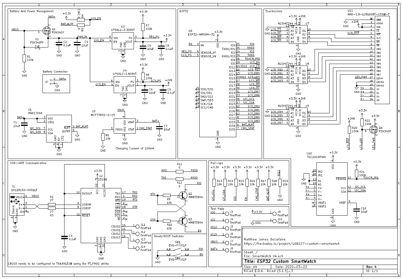
I made sure to put everything into blocks just to simplify the schematic a bit (and kept everything on one page). The most significant change from Revision 3 is the change from the ESP32 D4 Pico to the ESP32 WROOM module. Using the pre-built module allows for an easier design process and doesn't necessitate me routing any RF traces or dealing with any of the other black-magic that is WIFI radio. Switching to the module was a reluctant change on my part however, since the module occupies twice the boardspace of the D4 Pico. There's also the issue of soldering components together, and using the module will make hand-assembly marginally easier overall.
One major goal of this project is to have everything required by the smartwatch rolled into the smartwatch itself, so programming and charging need to be on-board and accessable by a USB connector. The rationale behind this is in line with the original project goal, this watch should be hackable on the fly and be able to perform any function it's hardware is capable of. The obvious cost of this being board space, so let's go through the board as it stands here.
From Revision 3 the USB-to-UART communication remains almost identical with the exception that this design uses the FT231XQ instead of the FT231XS. The only difference between the two IC's is the package, moving down to the QFN of the FT231XQ saves some board space for all the exciting new features.
Power Management Block
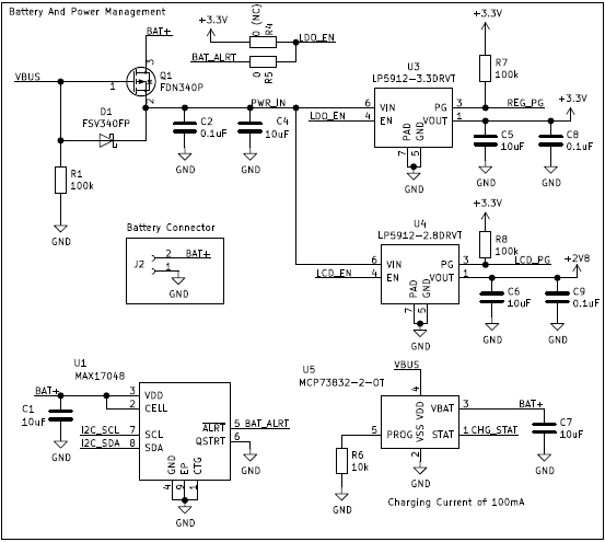
The power management block rolls together battery monitoring, charging, and regulation of the power. Starting from the upper left the circuit now selects between battery and VBUS when plugged into charge, this should allow the battery to charge without also being loaded by the operation of the watch itself. Two linear regulators are used to supply power to the circuit one supplying 3.3V and the other supplying 2.8V for the LCD. Battery charging is performed by the MCP73832-2 which charges at 100mA with a 10k resistor on the PROG pin.
The battery is monitored by the MAX17048 which is able to estimate battery percentage and shut down the regulators if a fault condition is detected. Information is fed back to the ESP32 which will handle most of the power management in normal operation. The regulator's power status and the MCP73832 charge status are also connected to the ESP32 allowing the software to know if one of the regulators drop out.
The dropout of the regulators in this design is a crucial feature, the 3.3V regulator drops out at 3.48V (in the absolute worst case) which is below the 3.6V maximum voltage the ESP32 can handle, this way the watch can operate all the way down to a battery voltage of 3.0V.
Touch Screen
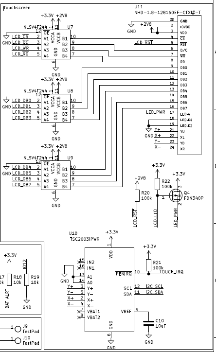
The touch screen itself is a 4-wire resistive touch screen with an 8-bit parallel interface. To support the touch functionality the TSC2003IPWR was selected to handle reading touch input. The TCS2003 communicates over I2C which was essential since every IO available on the ESP32 is already occupied. Another advantage to this IC is that we can use the PENIRQ pin to wake up the ESP32 in deep sleep mode. The TOUCH_IRQ pin connects to one of the RTC IO pins of the ESP32, allowing for the module to sleep until the screen is touched.
To support the 2.8V logic level of the touch screen all data traveling to the LCD moves through level shifters. For the level shifters this design uses the NLSV4T244 primarilly for their small form-factor to save board space. Finally the LCD's backlight is controlled by a single P-channel mosfet which is connected to the ESP32.
I may look for other touch screens, however this is the smallest I could find available from digikey.
Power usage
Since the last watch didn't go too great with power useage I decided to take a look at the design more closely before moving onto laying out the board. This won't be the most in-depth analsysis of the circuit but there is some good information contained here about the design.
To estimate the power useage of each component I used Excel to tabulate the power useage of each IC under various conditions of load (off, standby, active, and maxpower) and use these number's to estimate current draw over time.
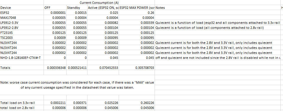
These values were obtained from the datasheets of the various components, but are not values that can be 100% relied on in some cases. More-or-less this excel sheet represents a "ballpark" of power useage. I plotted these current-use values in excel and obtained an estimte of power useage.
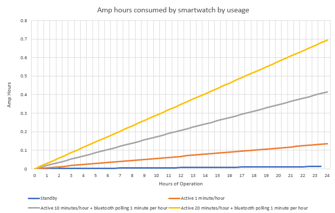
This assumes that "active" is the watch being used but not communicating over bluetooth or wifi. "bluetooth polling" assumes the watch is drawing the maximum power shown in the above table. Using this graph I can estimate the size of battery required for a given run-time of the watch, the previous design used a 300mAh battery which if used here would yield a battery life of anywhere between 10 and 18 hours depending on useage. I haven't fully decided on what size battery will be used in this revision but it'll most likely still be in the range of 300mAh.
That's everything I can think of to talk about in Revision 4. All that's left is to get the board made and start over on the software. See you in the next log!
Discussions
Become a Hackaday.io Member
Create an account to leave a comment. Already have an account? Log In.