 Alexis
By BP:
I’ve been working on the HPS/FPGA communication, and how we will handle buffering.
Architecture
I came up with this completed version of the architecture:
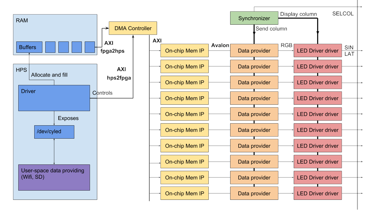
FPGA buffers will be fed by a DMA Controller. The DMAC will read data from RAM using the fpga2hps bus, and write to an AXI bus connected to all FPGA buffers.
On the HPS side, we will have a kernel module controlling the DMAC through the hps2fpga bus. It will be responsible of DMA transfer sequencing (between all buffers), and also the transfer timing.
The DMA source will be a pool of contiguous RAM buffers allocated by the driver.
Finally, the driver will expose a Linux char device. Through this device, a user-space app will be able to feed the buffers with data from various source (an SD card, a Wifi streaming).
Buffering
If you think about it, each half frame-slice will need to be printed twice, for it to be seen from all points of view. Thus, the drawing flow looks like this (where each line is a half turn, and the two numbers represents the frame being drawn by each half of the panel) :
- F(n, right) ; F(n+1, left)
- F(n+1, left) ; F(n+1, right)
- F(n+1, right); F(n+1, left)
- F(n+1, left) ; F(n+2, right)
- …
We can see that the first half always get data from the second half at previous round. Thus, if we swap buffers smartly across drivers, we can use half-a-turn buffers. This results in 3 buffers for 2 drivers storing (F(n), right), F(n+1, left), F(n+1, right)), where at each time, one buffer is useless and can be fed by the DMAC with the next correct half.
To start with simpler code, we will approximate to 1 buffer per driver (+33% data stored), with a full turn capacity. We will optimize only if needed, that is, if the throughput of the HPS -> FPGA is not sufficient to transfer that much data.
In RAM, we will have a double buffer. One where we write data for the next turn, and one with data that should be used during this turn.
Discussions
Become a Hackaday.io Member
Create an account to leave a comment. Already have an account? Log In.