 Tom
TomWhen opening the housing,
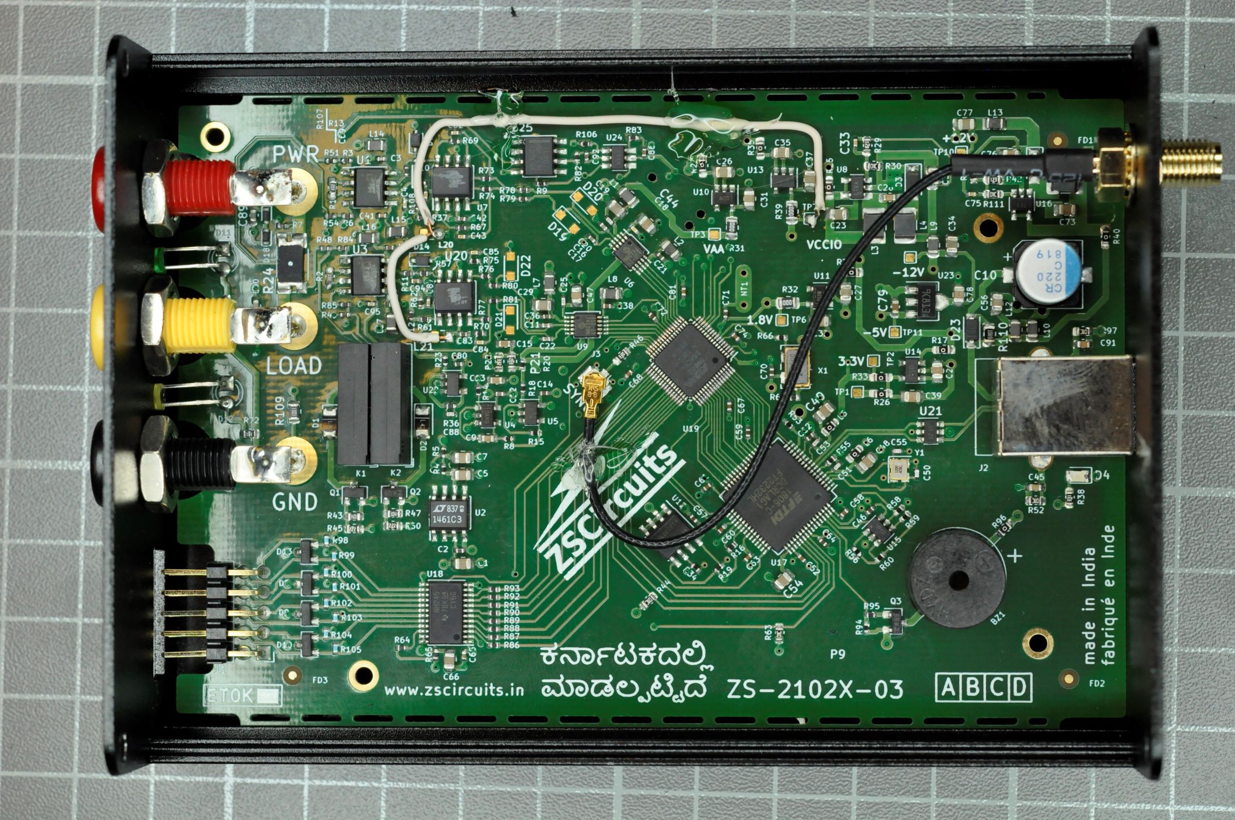
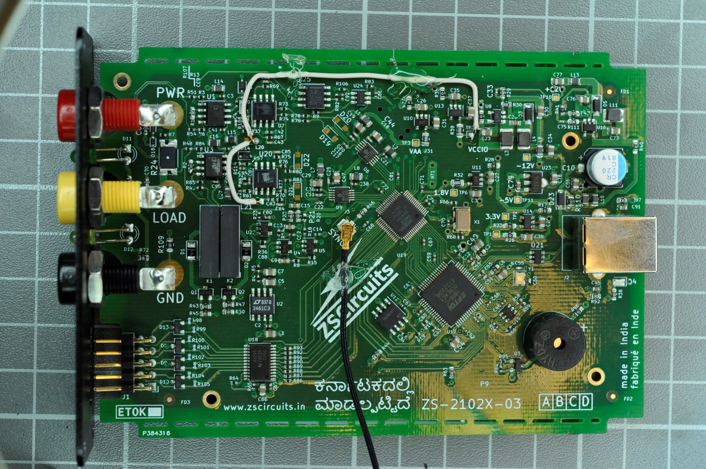
there are some eye-catchers:
- The part numbers of the instrumentation amplifiers and of the differential amplifiers are burnished away.
- The white wire which connects the negative supply of the differential amplifiers.
- There is no galvanic insulation between the USB port and the measurement circuit.
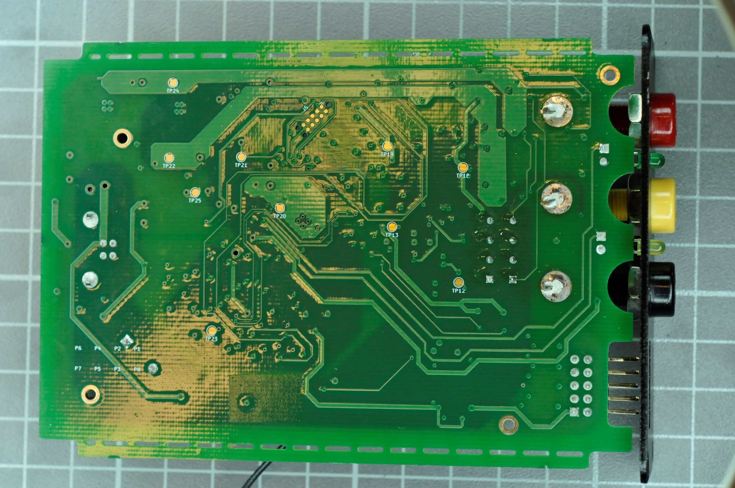
The PCB is assembled single sided, probably it is a 4 layer stack-up.
 Using a microscope i was able to read the part numbers of the burnished components. You find a list of the key components in the components list!
The clock output of the device is connected directly to the CPLD pin using a 33 ohm resistor.
From the hardware perspective this devices looks well designed with little discomforts:
- The 4mm banana connectors do have a very bad quality
- There is no galvanic insulation between the measurement circuit and USB
Discussions
Become a Hackaday.io Member
Create an account to leave a comment. Already have an account? Log In.
Nice! First thing I looked for was galvanic insulation and thought that maybe U21 was there for that purpose. Then read through it all.
- I think the bad banana plugs are not a "little discomfort". The connection to the outer world should be as reliable as possible with as little resistance as possible... Why cheap out on those parts?! This unit is 600USD!
- Scraping the top of your ICs is just bad. But fortunately they did it like they did their banana jacks :)
- The Kelvin connection of the current sense resistor looks far from how you do it "by the book". Especially those super long traces to the ADC/CSA. Routing would've been possible on the right side too?!
Edit: Please add the designator from the parts on the board when filling your component list. It's much easier for us to see where each part is on the board!
Are you sure? yes | no
Hi Jan :)
U21 is a TVS diode.
Several things are solved the cheap way and not the more expensive but elegant way.
You can always do things better ... ;)
I added the designators to the component list.
I just calculated the costs of the key components with about 35€ (30pcs batch).
Are you sure? yes | no