Close
0%
0%

An uninnovative linear LED display

16 LEDs in two columns, serially driven

Similar projects worth following
A LED display board that is versatile and cheap to fabricate

Background

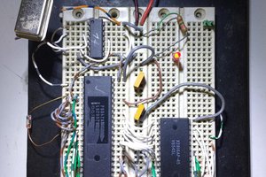
After finishing my TTL clock I was aware of limitations of that design. Not only are the chips old and would cost money to obtain (unless you have them in your junkspares box already) but they consume a fair amount of current (I measured about 70-80 mA for the LS TTL model). More serious is the reliance on the 32768 Hz crystal, which drifts, requiring adjusting the time now and then. That TTL clock design was only for my friends to brag how they have 30-40 year old ICs working in their clock.

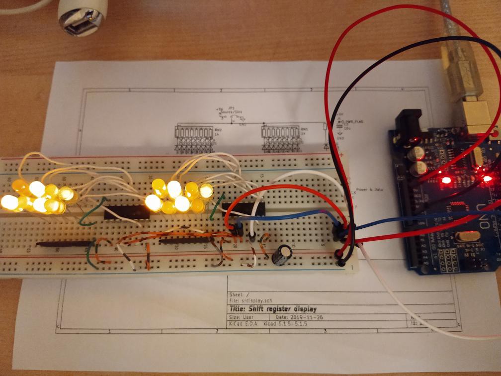
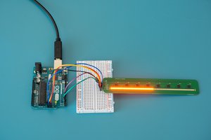
I could use a modern MCU to provide the timing, taking advantage of a corrected oscillator, an RTC board, or even sources like NTP or GPS. This would also consume less current and allow a better user interface. MCUs like the STM8 are very cheap. So what I decided to do is to partition out the display portion. The display would also be useful for other projects. Linear applies to the layout of the LEDs, not that it's an analog circuit.

Design

  • It should have a serial interface to minimise the number of interface lines
  • It should use easily available chips
  • It should be cheap to fabricate, ideally under 100x48 mm so that you can fit 2 on a cheap PCB
  • It should be versatile

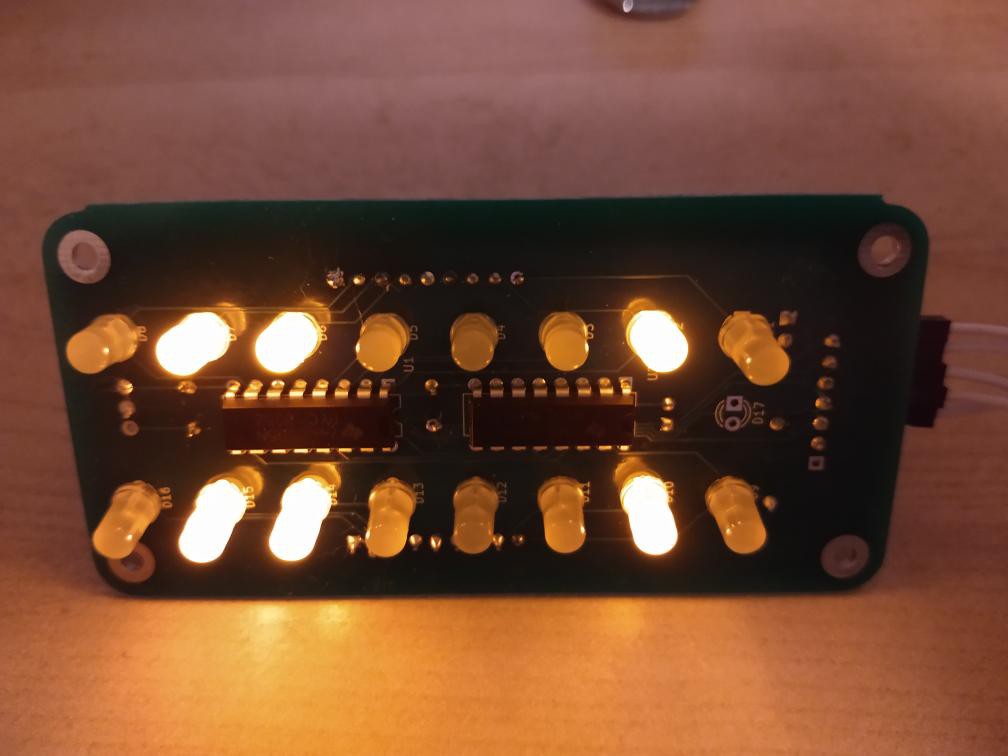
The obvious candidates for the chips are shift registers. The 74HC595 and the later TPIC6x595 are designed precisely for this kind of application. The latter is a power shift register and overkill, but the former is readily available and cheap.

The design is taken right out of the chip datasheets, hence the uninnovative. However I wanted to make it versatile. These are the things I have designed in:

  • You can populate as few or as many of the 16 LEDs as you need, although you still have to provide all 16 bits of data
  • There is no restriction on the mix of coloured LEDs used as long as they are happy with the voltage supply. But you may have to match efficiency for them to look roughly equally bright
  • The shift register is rated from 2V to 6V. Although the forward voltage of the LEDs means 3.3V is probably the lower limit. 5V works of course
  • The 74HC595 being CMOS is equally good at sourcing or sinking current, so you can source or sink current to the LEDs, selected by an assembly time jumper
  • You can optionally control the /OE line for PWM control of the brightness. This is jumper selectable
  • There is one optional LED 17 with a separate connection which you can use for other indications
  • The circuit fits in 100x48 mm so you can panelise 2 to a 100x100 PCB for cheap fabrication
  • A couple of resistor networks are used to reduce the footprint and soldering
  • You can orient the board horizontally or vertically as suits your project

So the minimum number of lines required to drive it, aside from the + and - power lines, is 3: DATA, CLOCK, and LOAD. The last is to strobe the data to the output registers so that you don't see the LEDs display the shifting data. The optional lines are: /OE for PWM, and LED17 for the extra LED.

srdisplay.pdf

Schematic

Adobe Portable Document Format - 62.55 kB - 11/28/2019 at 12:10

Preview
Download

  • Project completed

    Ken Yap01/02/2020 at 09:01 0 comments

    The boards have come back from the fab and I have assembled one, using the same components that were on the breadboard. Aside from one dry joint on one pin of a resistor network, everything works as before.

    So I'm declaring the project finished and I'll update the Github repo. I haven't got any places to use the boards yet.

  • Design released to Github

    Ken Yap11/28/2019 at 21:30 0 comments

    I have released the design files to Github rather than wait for a PCB. The PCB design is untested, but it should work (famous last words).

  • Doing the PCB fab rounds

    Ken Yap11/28/2019 at 02:14 1 comment

    Decided to try LocoPCB who support V-cut panelling of a single design for no extra charge. This to experience V-cut panelling and to write a review of my experience with them. LocoPCB also charges $2 for 5 boards, for the first 5 orders. Here is  ongoing story until the boards are received.

    Previously I checked PCBWay who is having an end of year sale so I decided to see if they'll do panelised PCBs, 2 per board, for the offer price. Unfortunately they want to charge extra for the slot, breaktabs, and mouse bites I put in. But I'll see if I can send another project in to take advantage of the offer.

    Then I checked JLCPCB who didn't object to a panelised board last order, and the normal price is good anyway. It turns out from reading their help page that JLCPCB have no extra charge for breaktabs and mouse bites provided it's a single design.

  • Getting the circuit working

    Ken Yap11/27/2019 at 05:37 0 comments

    As mentioned, the schematic is taken straight out of datasheets so I didn't expect any problems, nor did I encounter any. It was insanely easy to get working.

    After putting the components on a breadboard, and doing an anti-smoke accident check, I connected it up to an Arduino Uno to test it.

    Except for one LED plugged in backwards, which I corrected, the test program worked first time. Here it is:

    /*
       Test shift register display
    */
    
    #define DATA    2
    #define CLOCK   3
    #define LOAD    4
    
    void setup() {
      // put your setup code here, to run once:
      pinMode(DATA, OUTPUT);
      pinMode(CLOCK, OUTPUT);
      pinMode(LOAD, OUTPUT);
      digitalWrite(DATA, LOW);
      digitalWrite(CLOCK, LOW);
      digitalWrite(LOAD, LOW);
    }
    
    void writebyte(unsigned int i) {
      for (byte mask = 0x80; mask != 0; mask >>= 1) {
        digitalWrite(DATA, i & mask ? HIGH : LOW);
        delayMicroseconds(10);
        digitalWrite(CLOCK, HIGH);
        delayMicroseconds(10);
        digitalWrite(CLOCK, LOW);
        delayMicroseconds(10);
      }
    }
    
    void load() {
      digitalWrite(LOAD, HIGH);
      delayMicroseconds(10);
      digitalWrite(LOAD, LOW);
      delayMicroseconds(10);
    }
    
    void write2bytes(unsigned int i, unsigned int j) {
      writebyte(i);    // MSB
      writebyte(j);    // LSB
      load();
    }
    
    void loop() {
      // put your main code here, to run repeatedly:
      for (unsigned int i = 0; i < 256; i++) {
        write2bytes(i, i);
        delay(250);
      }
    }

    All that the program does is repeatedly display an 8-bit counter as binary on the two columns of LEDs in parallel, at the rate of 4 per second. This rather than display one 16-bit counter as I don't want to wait 5 hours to see the whole cycle.

    The CLOCK and LOAD lines are pulsed for 10 microseconds. This implies a maximum data rate of 50,000 bits/second, far more than adequate for this kind of display. I limit the rate so that the wiring isn't critical as it might be at a higher rate.

    Next step will be to get the board fabricated.

View all 4 project logs

Enjoy this project?

Share

Discussions

sunny wrote 02/02/2020 at 13:04 point

I assembled it, but I met some problems, I put. 2, 3, 4 and pin are connected to ser, rCLK and srclk. Is the connection correct? Then D10, 11, 15, 16 will light up in turn and then go out. It seems that the other LED should be on, but it doesn't work. The second chip has 5V input, but no corresponding output. JP1 and JP2 are connected to the schematic diagram. I don't know where the problem is. Also about the software, I modified the value of I in the loop part. It seems that it has no change to the LED output. Can you provide more information about the software, such as a document or several other examples. Thank you

  Are you sure? yes | no

Ken Yap wrote 02/02/2020 at 13:14 point

The circuit and program work as designed. I've tested both on a breadboard and on the PCB. Do not change the program until you understand the design. And make sure the LEDs are the right way around.

DATA goes to ser. CLOCK goes to srclk. LOAD goes to rclk. 16 bits are shifted in using DATA and CLOCK, and then the output buffer is updated instantly with LOAD so that the shifting is not seen.

In the schematic, understand the purposes of JP1 and JP2 and don't just accept the existing setting, that's just the default wiring of the symbol that Kicad uses. For JP1 the setting shown is correct for sourcing current to the LED. For JP2 If you are not driving /OE for brightness control with PWM, the jumper should be connected to ground, otherwise the outputs are in high-Z state so will not conduct in either direction (they are tristate outputs).

  Are you sure? yes | no

Dan Maloney wrote 11/27/2019 at 16:38 point

Datasheet scraping is a perfectly valid design method...

  Are you sure? yes | no

davedarko wrote 11/27/2019 at 13:33 point

You had me at "rounded PCB corners" ;D

  Are you sure? yes | no

Similar Projects

Does this project spark your interest?

Become a member to follow this project and never miss any updates