 Bud Bennett
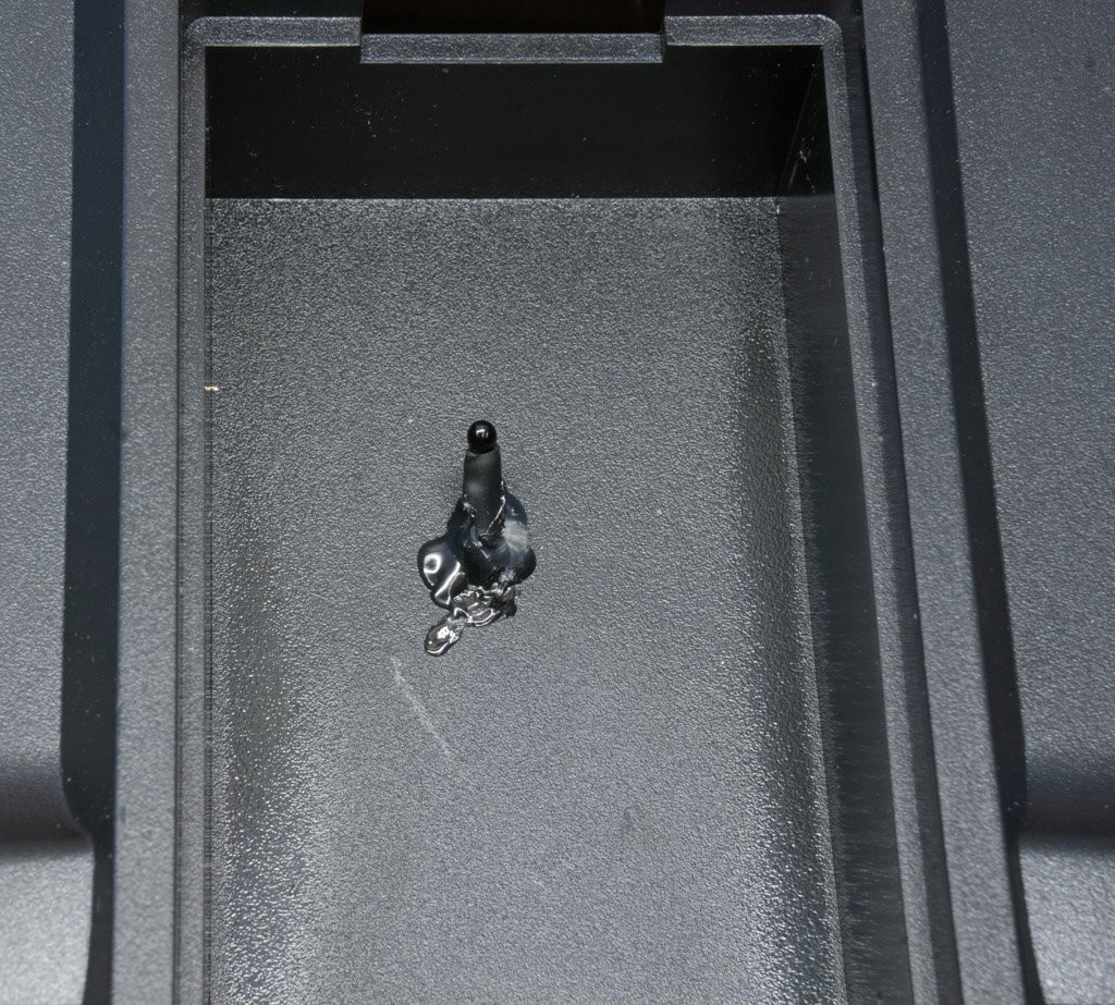
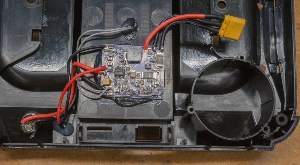
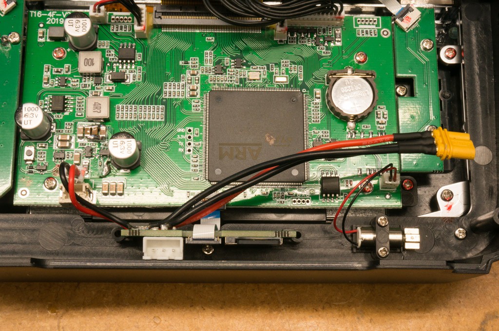
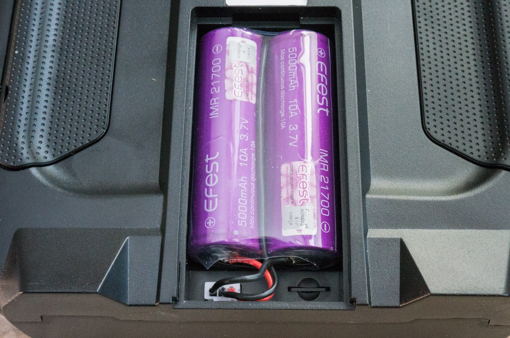
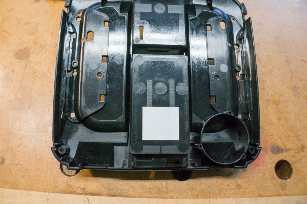
I was using a stack of 2 3.5Ah 18650 Li-Ion batteries to power the T16. They fit into the provided battery holder and a 3 terminal JST connector plugs into the back of the T16 to give it power. I've been using it so much that the batteries need to be recharged more than once per week. The battery compartment cover is tight and difficult to remove. I had to solder an XT30 connector onto the leads, in addition to the JST connector so that I could connect it to my RC battery charger and balance charge the two cells.
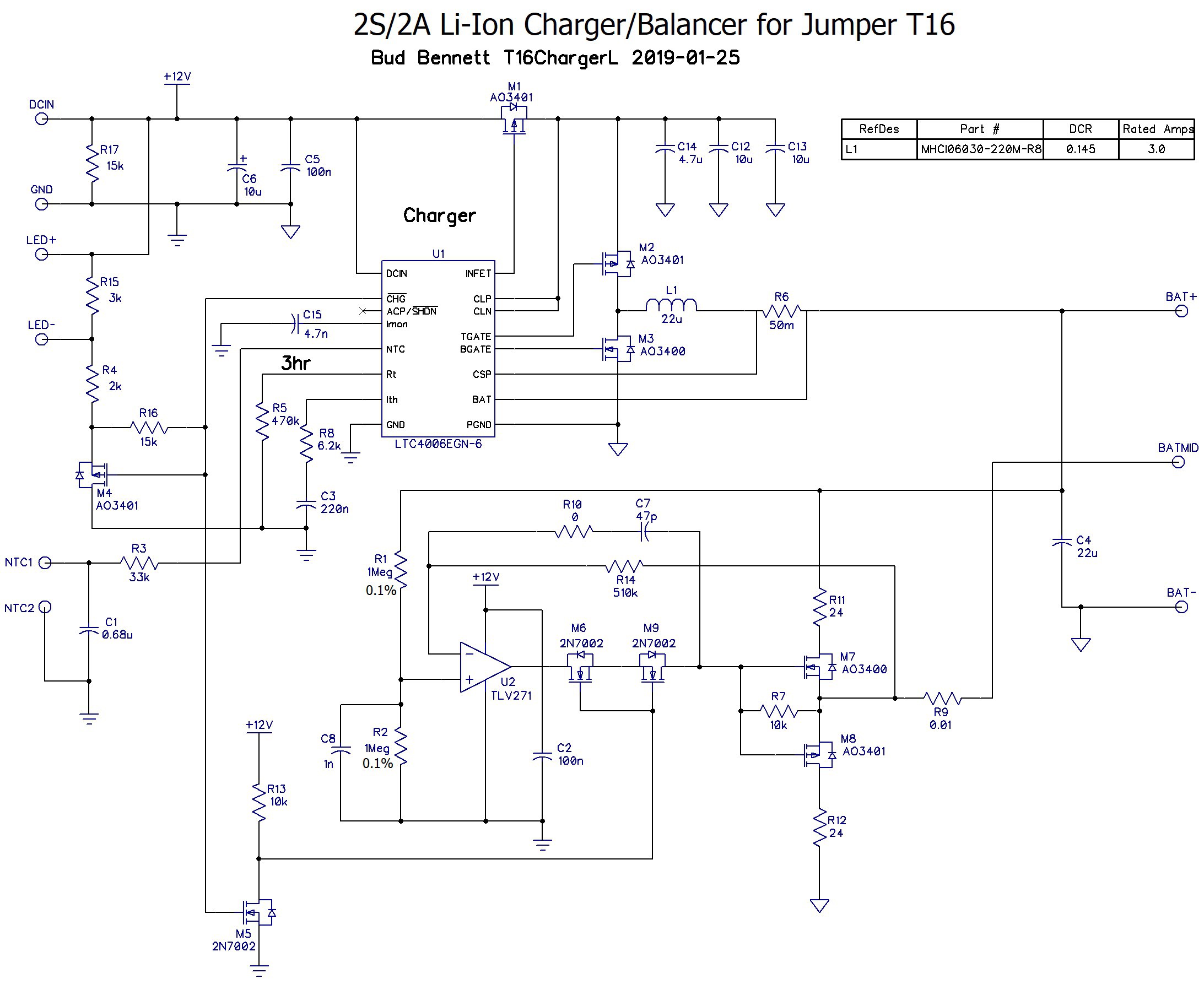
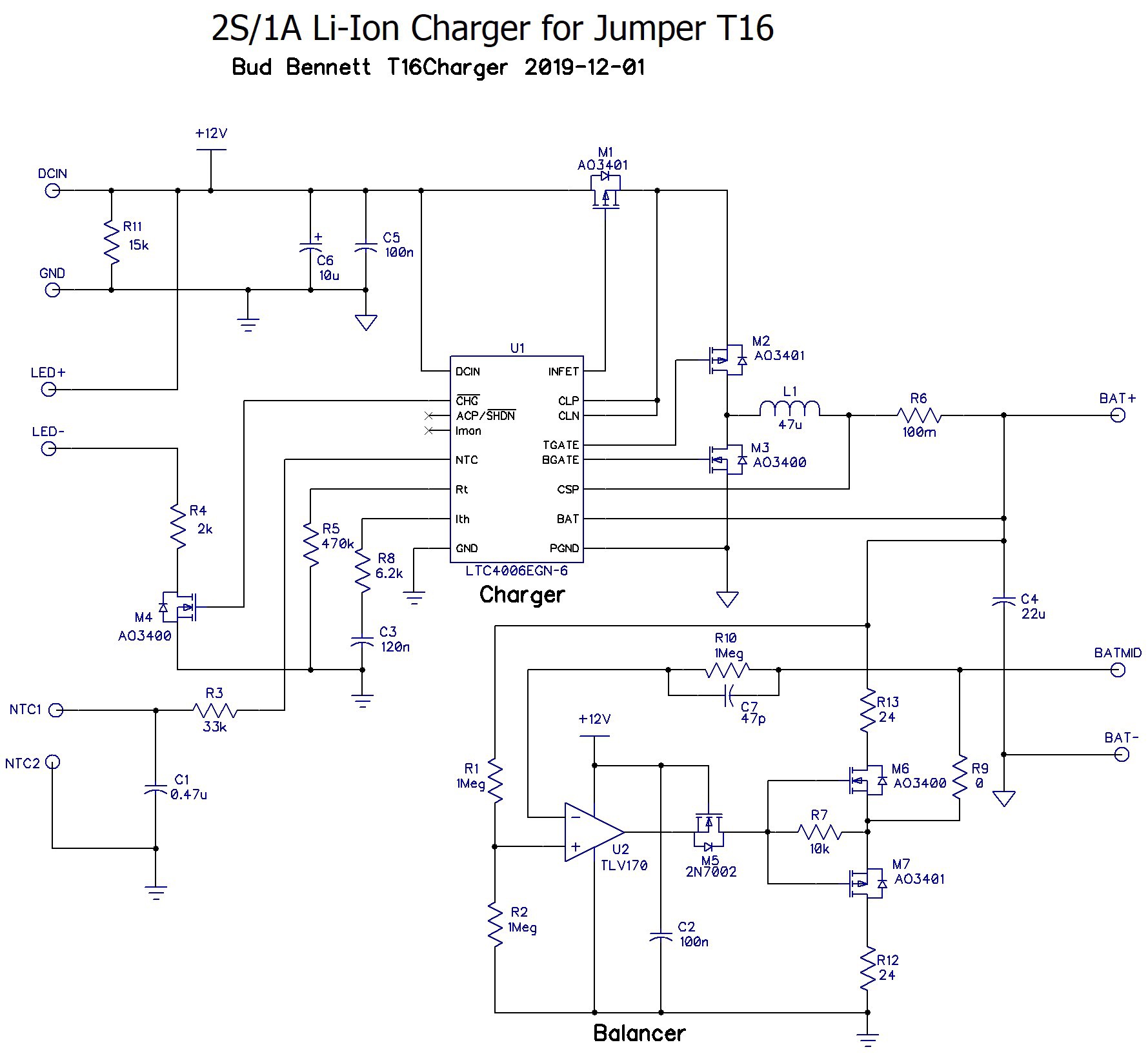
There has to be a better way. I'd like to just plug in a small barrel plug into the back of the radio and let it charge for a couple of hours automatically. The schematic below is what I've implemented:
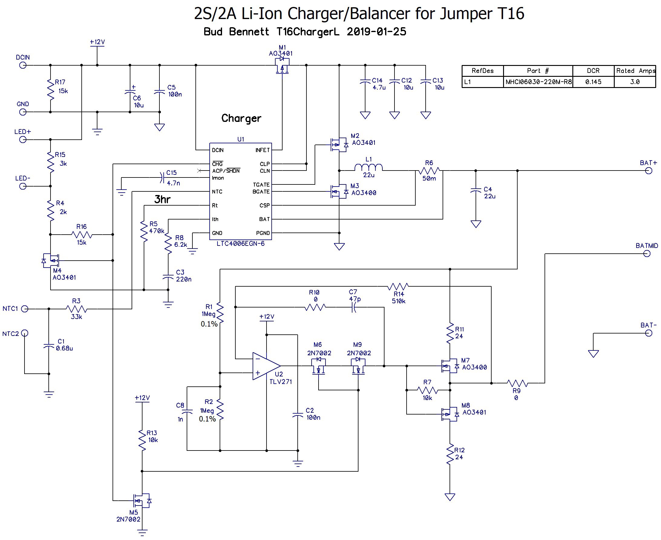
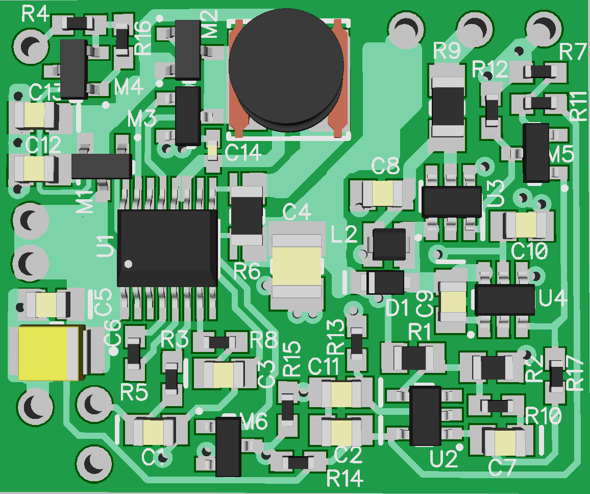
(Full disclosure: I designed the LTC4006 back in 2002. This is the first time that I've been able to use an IC that I designed in one of my projects.) The LTC4006-6, U1, is a stand-alone 2-cell buck-mode switching lithium battery charger. It contains a constant-voltage constant-current controller to charge the battery, along with a charge termination timer and a thermistor sensor interface to prevent charging the battery at unsafe temperatures. It is fairly efficient - 95%, so it should not dissipate a lot of heat inside the case.
The LTC4006-6 lacks a charge balancer, so I've attempted to provide that capability with U2 and associated components. The circuit attempts to hold BATMID at (BAT+ - GND)/2. It can source/sink up to 175mA into BATMID. Maximum power dissipation will be 0.75W, which will decrease the overall efficiency of the charger to 90%. I expect it to get relatively hot.
The balancer circuit operates until the current from the charger drops below 10% of the programmed current. Then the CHG_ pin drops below 25µA and then it is dragged upward by the LED and resistor loads — turning off the LED. This causes M5 to disable the balancing circuit and M6 & M9 to disconnect it from BATMID to prevent current drain on either battery. After the LTC4006's timer expires it will go to standby mode until the user disconnects the power.
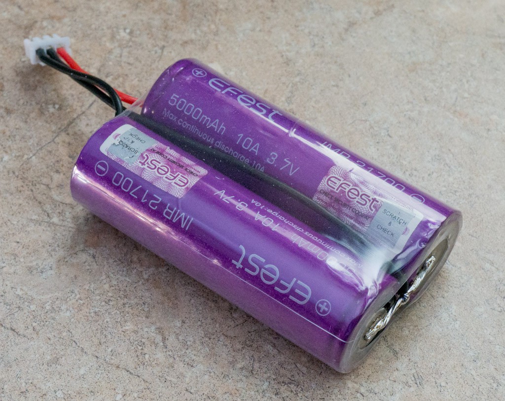
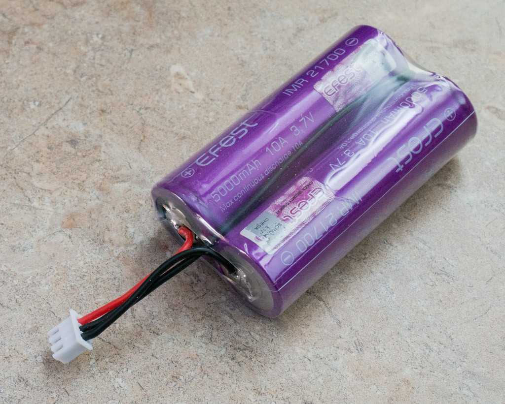
I have upgraded the battery pack to a 2S1P Li-Ion stack of 21700/5Ah cells, which should yield longer battery life, but barely fit in the battery compartment of the T16.
The charger will be powered by a 12-15V AC/DC adapter capable of providing >1.5A. I've got a few of those lying around.
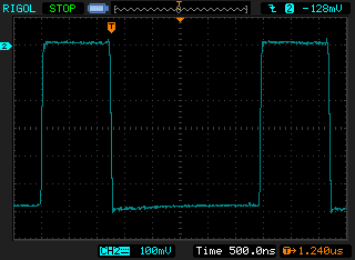


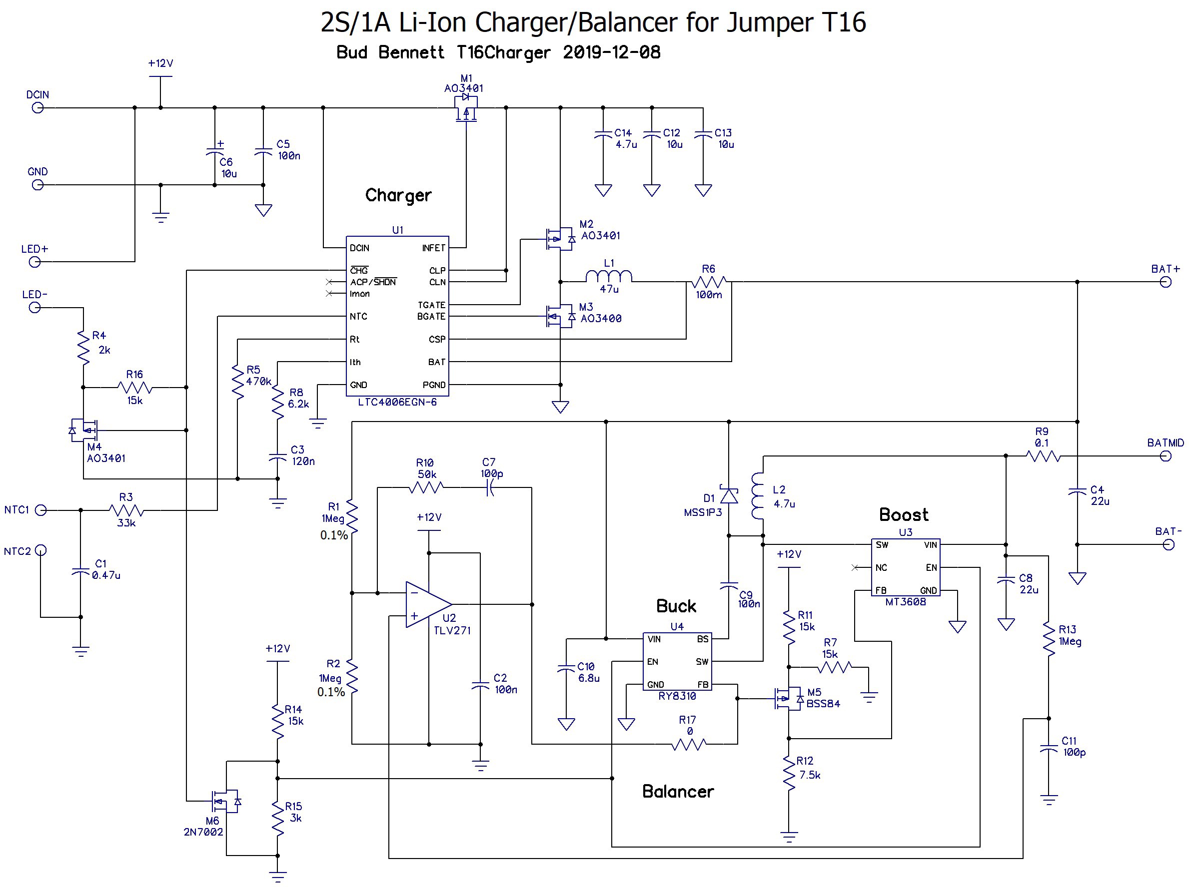
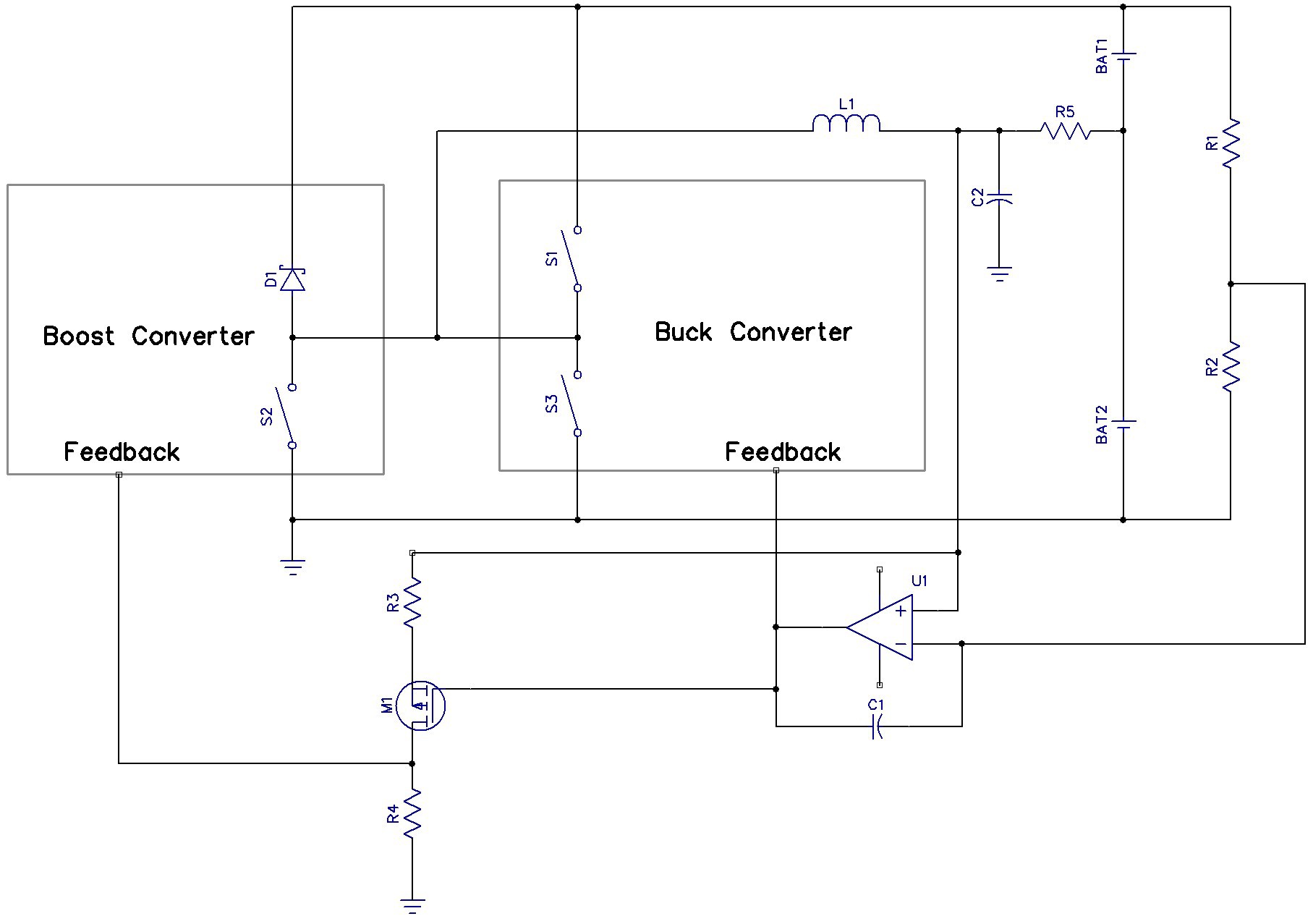
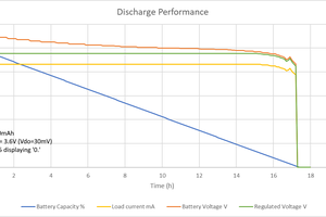
 The batteries are emulated with large capacitors -- C2 and C3. I offset the initial voltages on the batteries and unbalanced them by 10% in capacity. Initially, the lower battery has a lower voltage and also a lower capacity. The charger is just a 1A current source, I1. As the batteries charge the capacity imbalance will cause the voltage on the lower battery to exceed that of the upper. When the balancer begins operation it turns on the buck converter to take charge from the upper battery and put it on the lower. You can see the current through R1 (the upper trace) start out relatively high and then scale back as the batteries equalize. The buck converter goes into burst mode as the current decreases until it stops operation altogether when the batteries are equal. Eventually, the voltage on the lower battery gets bigger than the upper battery because it has the lower capacity and will charge faster than the upper battery. When this happens the boost converter turns on to remove about 50mA from the upper battery and send it to the lower battery to keep them charging evenly. You can see the two feedback inputs to the converters (the middle traces) switch over when this happens.
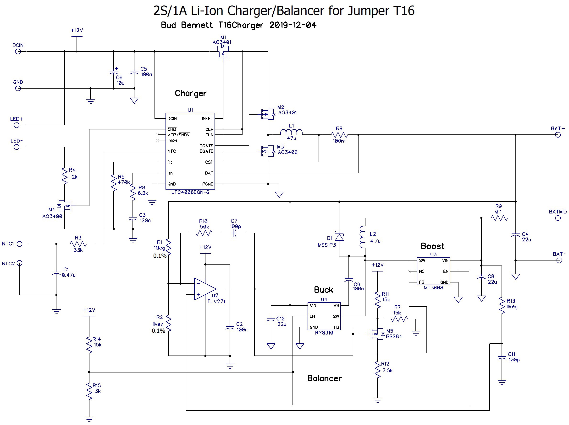
 George
 Sagar 001
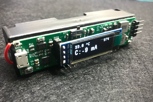
 Manuel Alfonso
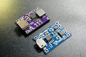
I got my TX18s, door not sticky, takes around 400mA with backlight on max.