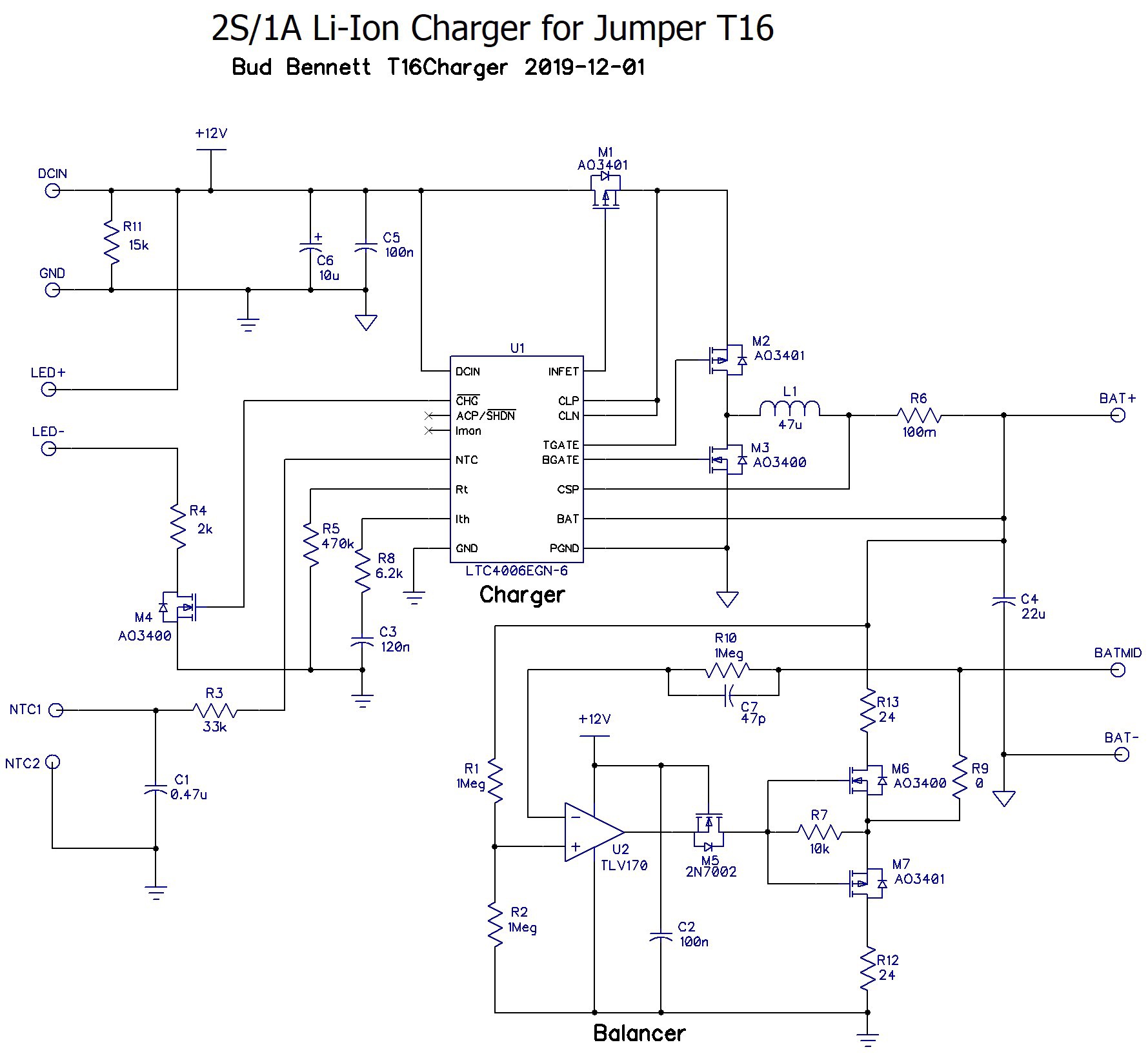
 Bud Bennett
My first approach to a balancing circuit is the schematic below.
All it does is source or sink a current into the battery stack to attempt to equalize the voltage across each battery. R12-R13 limit the current into the batteries to about ±250mA. They are large 1W resistors to avoid smoking with the 0.75W max dissipation. I thought that there might be a better way. There are a couple of YouTube videos that talk about a small circuit that would equalize a battery stack with up to 1.2A, using a switched-mode circuit. You can get one from AliExpress for a few $$. The problem with that circuit is that it only balances errors greater than 100mV -- reducing them to 30mV.
A crazy idea:
After a couple of days of mulling it over in my head, and then another couple days simulating it on LTSpice, I came up with this concept of a switched-mode battery balancer.
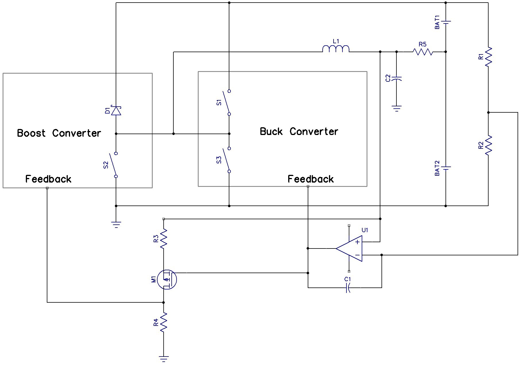
It's kinda brute force. The easiest way to think about how this circuit works is that the buck converter sources current through the inductor, and the boost converter sinks current through the inductor. If BAT1 has more voltage than BAT2 then the buck converter operates to take current from BAT1 and give it to BAT2 until the voltages equalize. Conversely, if BAT2 has more voltage, the boost converter operates to remove current from BAT2 and route it to BAT1. The opamp, U1, senses when the batteries are out of balance and directs the converters to source or sink current appropriately. Only one converter can be active at a time -- this is insured by the simple inverter using M1. This only works if there is an amount of resistance in the batteries, or added by R5, that will limit the current from the converters.
I was able to simulate the operation of the circuit using LTSpice. I used Analog Devices converters since they provided the models for them in LTSpice.
 The batteries are emulated with large capacitors -- C2 and C3. I offset the initial voltages on the batteries and unbalanced them by 10% in capacity. Initially, the lower battery has a lower voltage and also a lower capacity. The charger is just a 1A current source, I1. As the batteries charge the capacity imbalance will cause the voltage on the lower battery to exceed that of the upper. When the balancer begins operation it turns on the buck converter to take charge from the upper battery and put it on the lower. You can see the current through R1 (the upper trace) start out relatively high and then scale back as the batteries equalize. The buck converter goes into burst mode as the current decreases until it stops operation altogether when the batteries are equal. Eventually, the voltage on the lower battery gets bigger than the upper battery because it has the lower capacity and will charge faster than the upper battery. When this happens the boost converter turns on to remove about 50mA from the upper battery and send it to the lower battery to keep them charging evenly. You can see the two feedback inputs to the converters (the middle traces) switch over when this happens.
Making it Real:
I found several switched-mode converter ICs for a lot less than what Analog Devices wanted to do the job. Here's my first attempt at a real solution for a SMPS battery balancer:
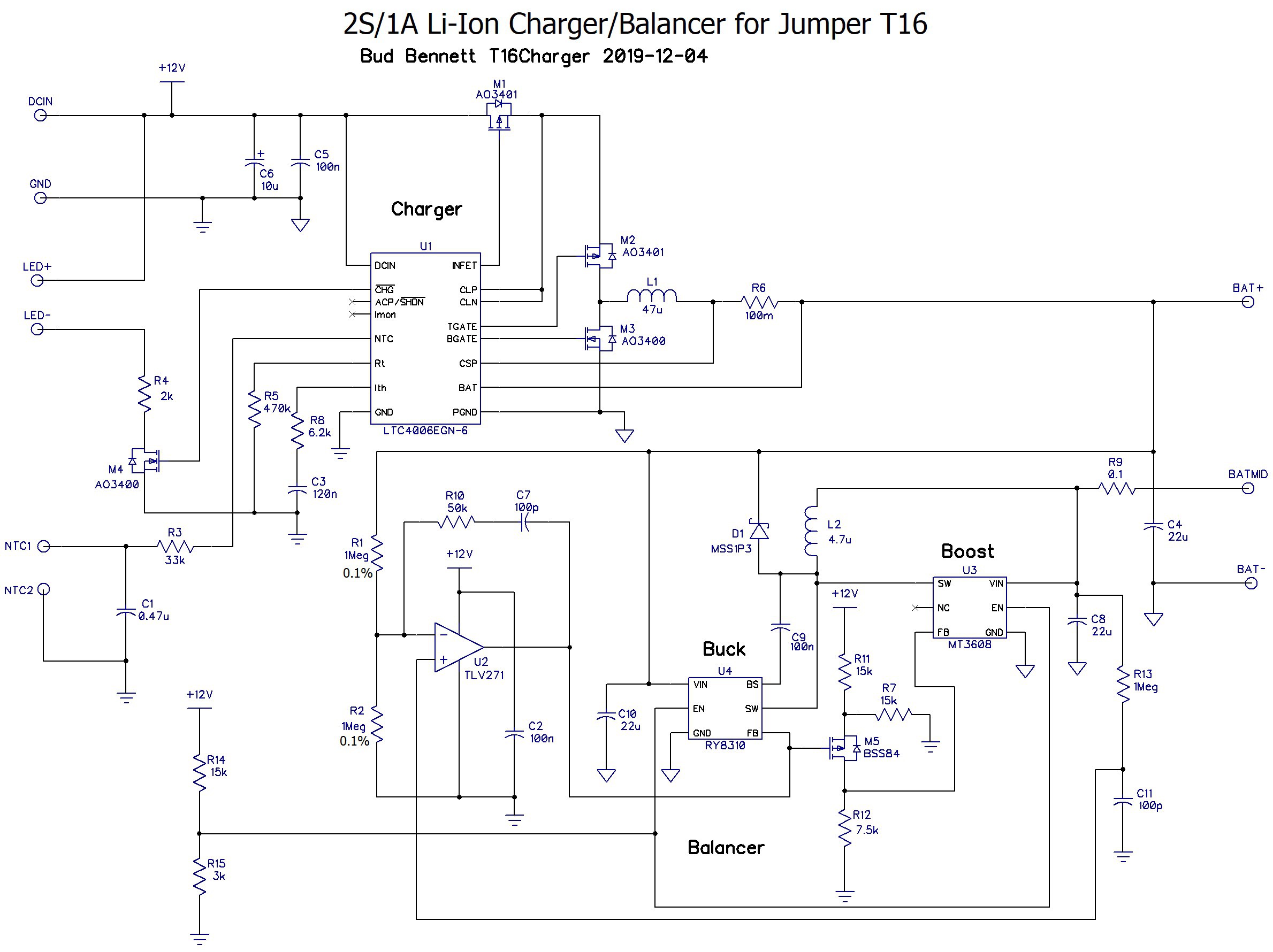
U3 and U4 are SOT23-6 switchers operating around 1.5MHz. L2 is a small, 2.0x1.6x1.2mm inductor that is shared between the two switchers. R9 sets the maximum current sourced/sunk by the switchers. I decided to use 0.1% tolerance resistors, R1-R2, to set the balancing voltage of the stack. If I were to use 1% tolerance resistors the error between the two battery voltages could be above 80mV. With the better tolerances, the balancing error should be below ±10mV.
The last design consideration is the leakage current out of the batteries after the charging event. The LTC4006 specifies a current drain from the battery less than 15µA. Other leakage sources are R1-R2, R13, U3-U4 shutdown current, and the reverse leakage of D1, which is specified as 1µA typical @ ~5V. Summing all of the potential leakage sources together yields a total current drain from the batteries of around 30µA. I calculate that 30µA would drain the stack by 0.15V over the course of one year. That's acceptable.
The next step is to layout the PCB and compare the size/cost of the two approaches.
Discussions
Become a Hackaday.io Member
Create an account to leave a comment. Already have an account? Log In.