 Bud Bennett
I'm switching back to the linear balancer for three reasons:
- There is no current limiting. If two discrete batteries are loaded into the battery holder the voltage difference between them could cause the switching balancer to put out more than 1.2A. I could not find an inductor, L2, in a 2mm x 1.6mm package that could withstand that current for very long. I had already smoked to L2 inductors while debugging the first prototype.
- I don't really understand how the buck and boost ICs are reacting to being driven in an unusual manner. They get hotter than I expected. The whole point of using a switching balancer was to decrease power dissipation and that did not appear to be happening.
- The max power dissipation of the linear approach is 0.75W and the balancer circuit is current limited. The additional power dissipation decreases the efficiency of the overall charger to 90%, which is probably acceptable, but that is 1.7W!
An updated linear balancer schematic:
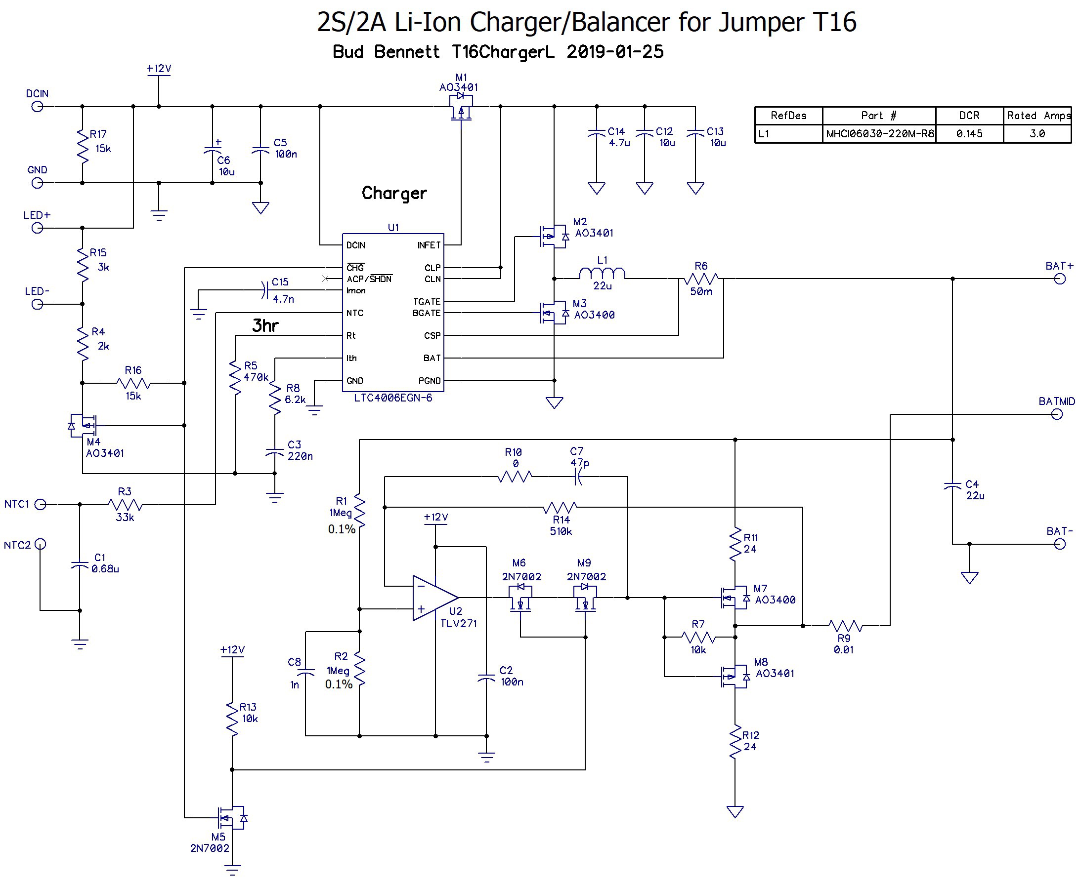
The charger circuitry did not change. I simulated the balancer and came up with a few changes to improve stability. It is just a voltage follower with a current limiting output stage. In operation, M5 is turned off by CHG_ and M6 & M9 connect U2 to the output stage, M7-M8. U2 will attempt to force BATMID to be (BAT+ - GND)/2 with a current of up to 175mA, limited by R11 or R12. R11-R12 are 2512 size resistors rated at 1W. The maximum power dissipation of M7 and M8 will be 0.2W, which is well within their rating.
Compensation to prevent oscillation is provided by C7 and R10. C8 provides filtering at the input to reduce any 300kHz switching noise from the charger.
When CHG_ goes high, indicating the the charger current has dropped below 10% of programmed current, the balancer is turned off by taking the gates of M6 & M9 to GND. This disconnects the output stage and it will float with very little current flowing -- nA. U2 won't like this and its output will be indeterminate, which is why M6 & M9 are connected with their sources together and will prevent any current flow to the gates of M7-M8 no matter what voltage is at the output of U2. When DCIN is disconnected the gates of M6 & M9 are near GND and the balancer is off. There will be some leakage current from R1 and R14 connected to the batteries and U2, but it will be just a few µA.
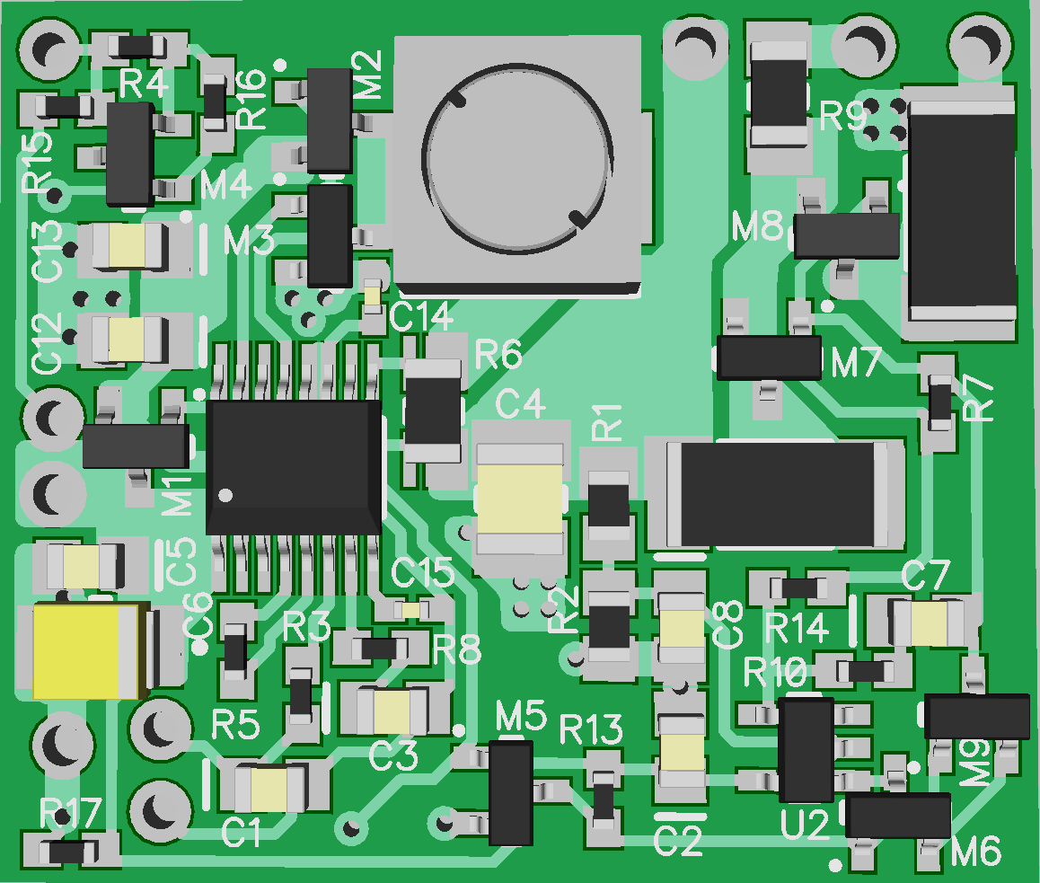
The layout is the same size as the switching balancer -- about 1.0" x 1.2" -- $6.05 for 3 PCBs from OSH Park:
Discussions
Become a Hackaday.io Member
Create an account to leave a comment. Already have an account? Log In.