 schwarzrmsu
In my previous project log I developed a function to read the key pad. In this function there were some necessary delays in order to allow the digital output to fully charge the capacitor on the digital input filter before checking the digital input status (check out more details on the keypad in my previous project log). This delay is based on the RC time constant of the RC low pass filter I have placed in front of each digital input for the key pad.
Below is a visual example of whats happening in the circuit:
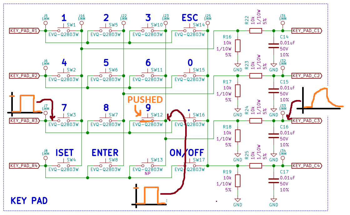
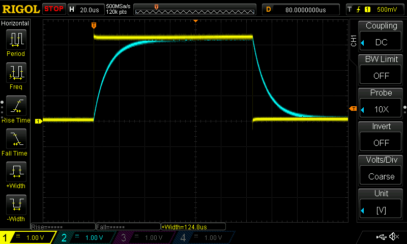
You can see that the signal at TP7 and TP23 are instantaneous because there is no deliberate capacitance tied to that node. Therefore the rise and fall times are going to be "instantaneous". The problem is the signal at the digital input is not "instantaneous" because of the resistance/capacitance combination. This resistance/capacitance combination is called a passive low pass filter. Its a cheap and effective way of filtering out unintended high frequencies that you do not want present at your digital input. These high frequencies can come from a number of sources, but typically it is outside RF being coupled into the trace acting like an antenna.
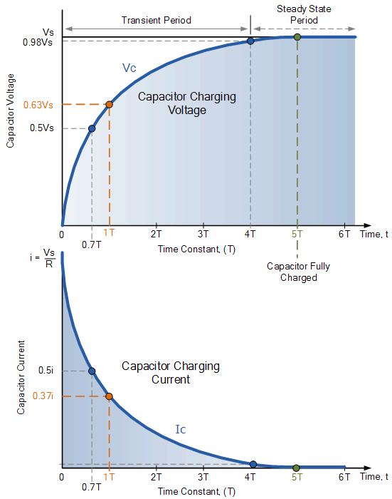
In order to use this low pass filter, we need to wait for the signal to catch up before we read it. This time is based off the RC time constant of the low pass filter. The RC time constant formula is below:
For our circuit we have to consider R as the two 10k resistors, and C as the 0.01uF capacitor. It is best practice to use the worst case value when running an analysis to ensure its compatible across all possible conditions. For this scenario the worst case condition is at the maximum resistance & capacitance values. Our maximum component values are calculated below:
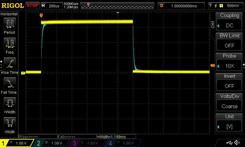
Unfortunately 1T is not enough time since that will only allow the voltage to reach 63% of the steady state value. Its best to wait at least 5T in order for the capacitor in the low pass filter to fully charge before reading the input. This is shown best in the figures below:
Therefore the delay we need to wait after each row is powered is calculated below:
I rounded this value up to an even 1200us and tested the response:
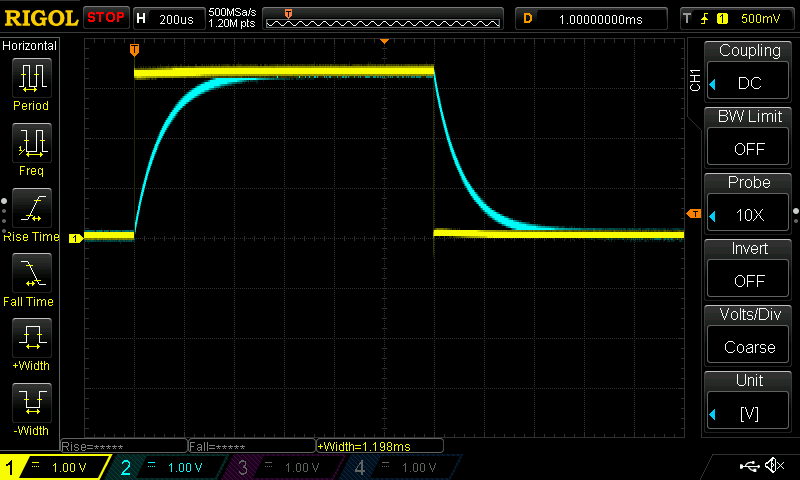
Here you can see the Digital Ouput Voltage (CH1) is instantaneous and the voltage at the Digital Input (CH2) has reached its steady state. This is exactly what you want to see in order to ensure the voltage you we monitoring has reached its steady state.
The problem is this takes place 4 times during the readKeyPad() function which gives us a worst case function delay of ~4.8ms. I measured this by executing the following code and taking a measurement on the green LED control:
     if (mainMillis - readKeyPadMillis >= 10)
      {
          turnOnGreenLED();
          readKeyPad();
          turnOffGreenLED();
          readKeyPadMillis = mainMillis;
      }
This function will set the green LED control high, run the readKeyPad() function, and then set the green LED control low. I did this an probed the green LED control to measure the time it takes to execute this function:
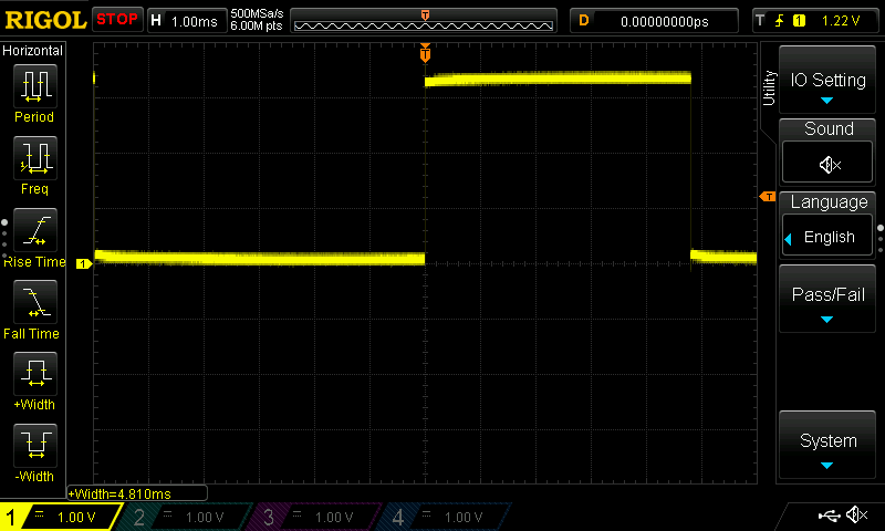
As you can see, it takes 4.81ms to execute the readKeyPad() function. This is too long in my opinion, therefore we need to make some HW changes in order to reduce the delays required for this feature. We either need to reduce the low pass filter resistance or capacitance in order to reduce the RC time constant which directly correlates to the required delay. This will move the corner frequency of our low pass filter, but this trade off is definitely worth it. I decided to keep the resistance the same, but to replace the 0.01uF capacitors with 0.001uF capacitors:
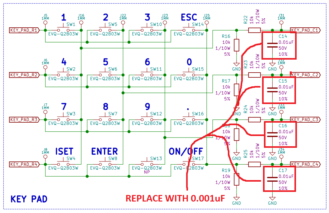
First we had to find C14, C15, C16 & C17 on the PCBA:
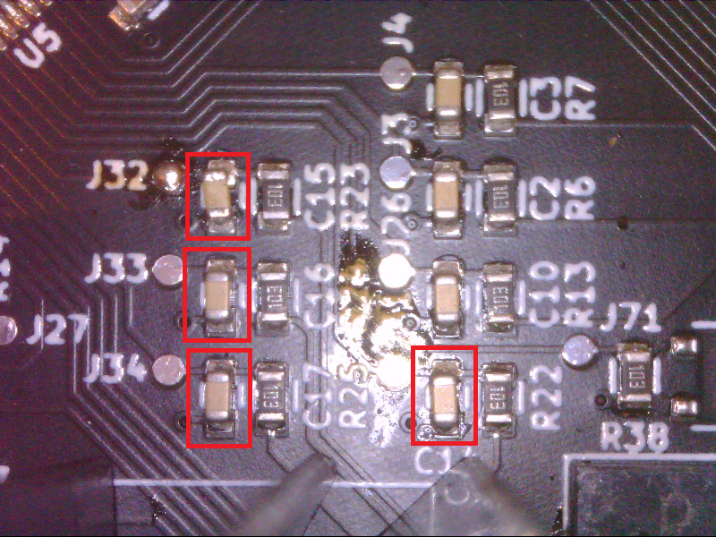
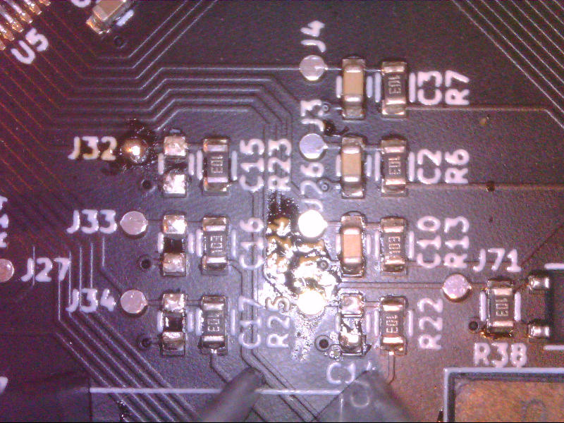
Remove these capacitors from the PCBA:
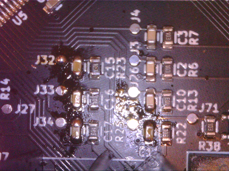
Solder 0.001uF capacitors:
Below is a waveform with the same delay but new capacitors:
You can see that the 1200us of delay for each digital output is now much longer than we actually need. I adjusted the delay in the SW from 1200us to 120us for each output and go the new response:
I reran the same test to measure the overall function delay and got the following result:
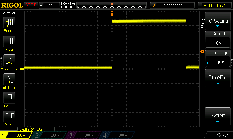
Now the function only take 511uS to execute, which is much more acceptable.
I hope you enjoyed my post. Thank you for reading. Please feel free to leave a comment below.
Thanks again.
Discussions
Become a Hackaday.io Member
Create an account to leave a comment. Already have an account? Log In.