 Gerriko IO
Introduction
NXP describes the PN7150 as a high-performance version of the PN7120, which is a plug’n play NFC solution for easy integration into any OS environment, reducing Bill of Material (BOM) size and cost compared to say the pin compatible PN532 controller. It provides direct connection to the main host (MCU or MPU) by I2C-bus and the NCI 1.0 communication protocol.
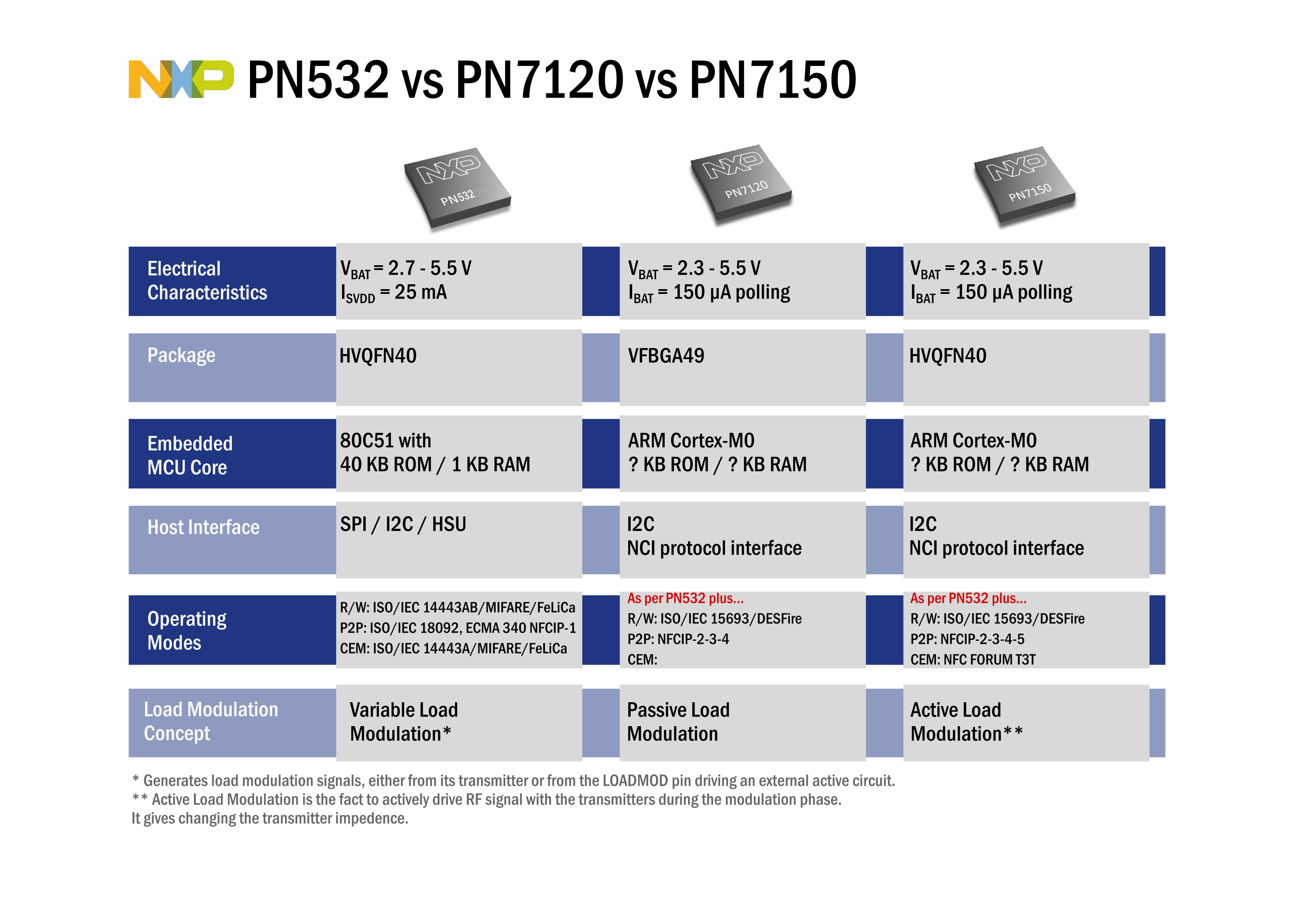
Like the older PN7120, the PN7150 has an embedded Arm® Cortex®-M0 microcontroller core, which is loaded with integrated firmware, supporting all NFC Forum modes for contactless communication at 13.56 MHz. This simplifies application development and implementation as all the NFC real-time constraints, protocols and the device discovery (polling loop) are processed internally.
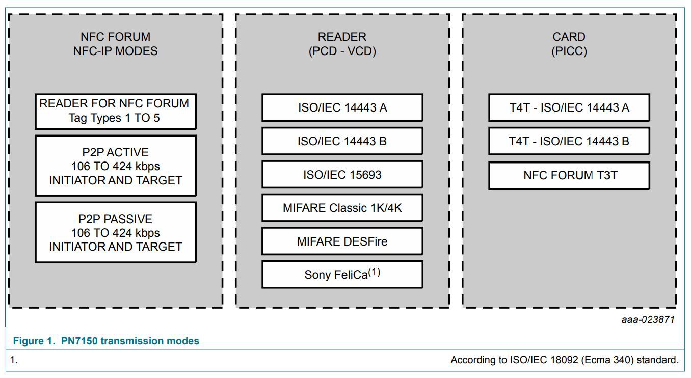
The PN7150 embeds a new RF contactless front-end supporting various transmission modes according to NFCIP-1 and NFCIP-2, ISO/IEC 14443, ISO/IEC 15693, MIFARE Classic IC-based card and FeliCa card specifications.
The NXP Single Board Computer (SBC) Demo Kits
NXP have 3 configurations of it's PN7150 NFC Controller SBC kit:
- OM5578/PN7150ARD for Arduino R3 boards
- OM5578/PN7150RPI for Raspberry Pi
- OM5578/PN7150BBB for BeagleBone Black/Green/Blue
Another useful PN7150 reference design is the Mikroe NFC USB DONGLE. However, the antenna on the Dongle is a much smaller size and so the matching circuit used is different.
For the purpose of this project, the OM5578 Interface Board, which sits on top of the SBC kit, will be used as the reference design as the antenna shape and size conveniantly fits within a FeatherWing Tripler protoboard.
Besides the data sheet and the user manual, NXP provide two very useful application notes, which help guide the design elements:
- AN11756: PN7150 Hardware Design Guide
- AN11755: PN7150 Antenna Design and Matching Guide
OM5578 Hardware Design Review
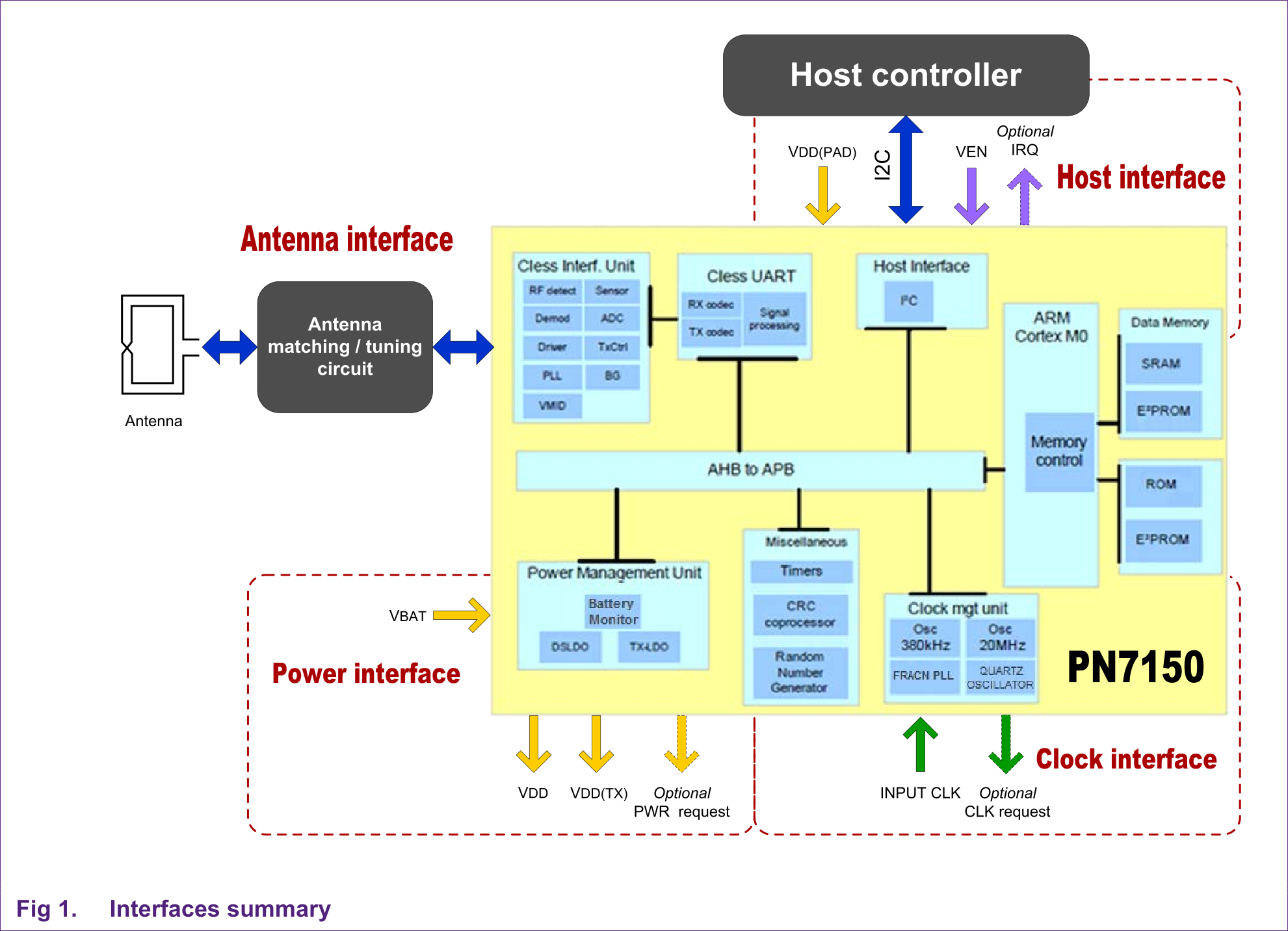
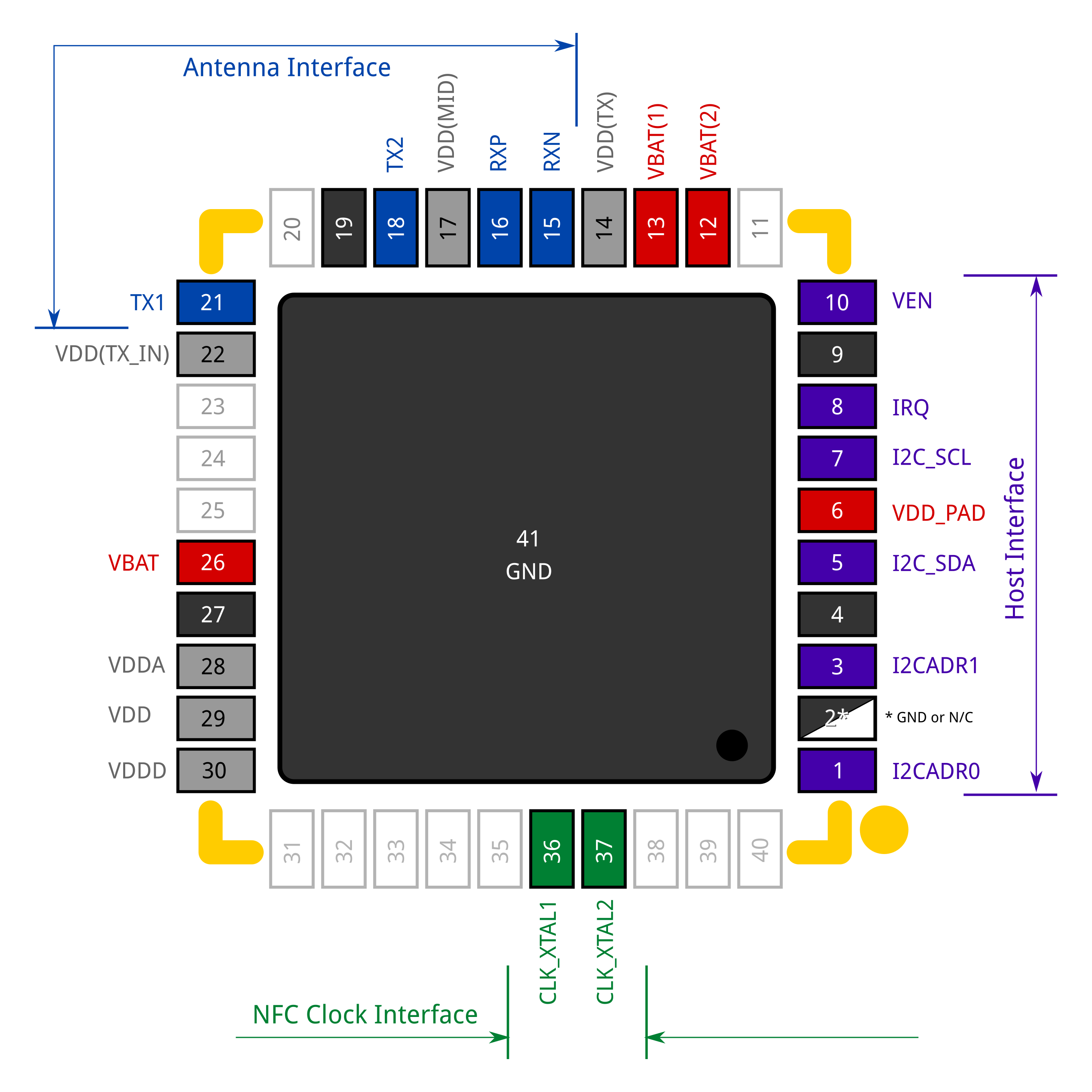
PN7150 Host Interface
There are 4 possible I2C slave addresses for the PN7150. These are set as follows:
| I2C Address (R/W) | I2CADR0 (pin1) | I2CADR1 (pin3) |
|---|---|---|
| 0x50/0x51 | 0 (GND) | 0 (GND) |
| 0x52/0x53 | 1 (VDD_PAD) | 0 (GND) |
| 0x54/0x55 | 0 (GND) | 1 (VDD_PAD) |
| 0x56/0x57 | 1 (VDD_PAD) | 1 (VDD_PAD) |
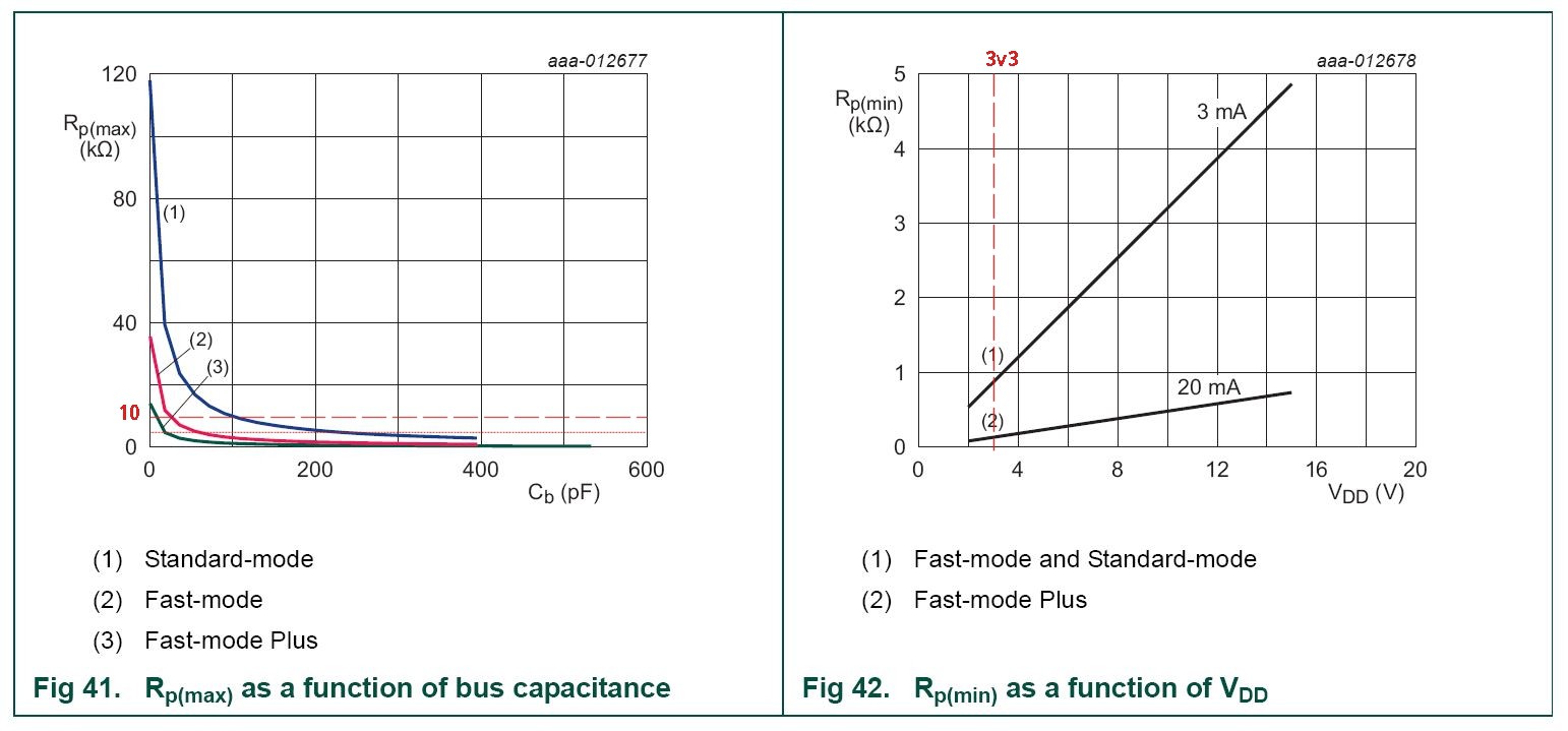
I2C Pullup Resistors are required. These were not included on the OM5578 interface board, so these will be be added into this design. The values of these resistors can be determined using NXP's I2C bus specification and user manual (UM10204).
For this design, 4k7 resistors were chosen on the assumption that Standard-mode (100k) is used as default. As the circuit if pretty compact, one could assume that the bus capacitance is below 100pF for Fast-mode (400k) to work too.
The hardware design document (AN11756) recommends that the IRQ pin is connected as an external interrupt to the host controller. The PN7150 IRQ signal can be configured active high or active low via the NCI Configuration API. This configuration is stored in non-volatile memory. The IRQ signal will be active any time data is available in the PN7150 send buffer. The IRQ pad state is maintained during the standby mode and is configured as pull down in hard power down mode.
The VEN pin is used to reset or activate the PN7150 chip. When VEN is greater than 1.1V the PN7150 chip is powered from VBAT. When the VEN pin is pulled lower than 0.4V, the PN7150 is in a hard powered down state. The chip is reset when VEN is switched back to a voltage level higher than 1.1V.
PN7150 Clock Interface
The 13.56MHz RF field carrier accuracy requirements are not compatible with the use of an internal oscillator, which can be found within the PN7150 ARM Cortex M0+. An external 27.12MHz crystal needs to be used as the input clock for PN7150, which is attached to the XTAL pins.
The following crystal oscillator have been properly checked by NXP as suitable for use:
- NDK NX2016SA 27.12MHz EXS00A-CS06346
- NDK NX2016HA 27.12MHz EXS00A-CH00075
- Murata XRCGB27M120F3M10R0
PN7150 Power Management Interface
The PN7150 can operate within a voltage input range from 5.5V down to 2.75V and can be directly connected to a battery power supply via VBAT.
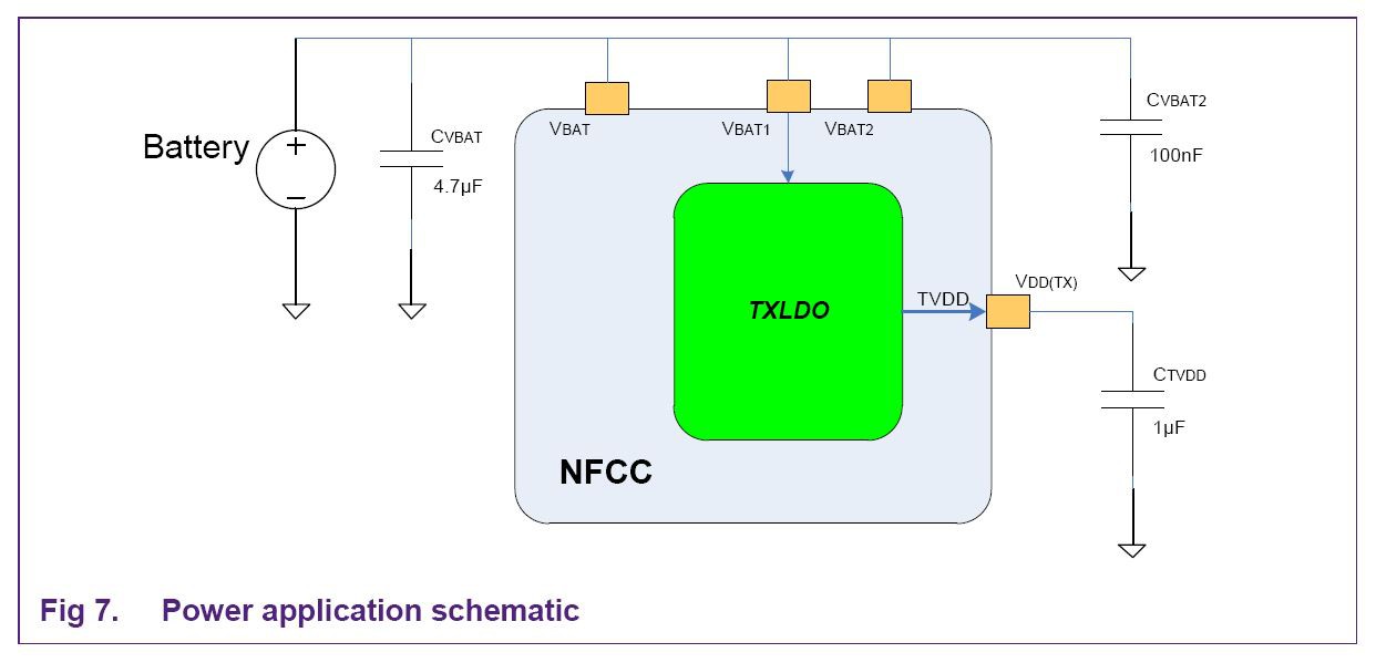
There are two LDO's within the PN7150 power management architecture.
There is the DSLDO which generates the VDD required for the PN7150 core. The input supply voltage for the DSLDO regulator is the VBAT pin.
The other is the TXLDO, which provides a current load up to 180 mA. The input supply voltage to this LDO regulator via the PN7150 VBAT1 pin.
The VBAT2 pin is referred to as the battery supply voltage and according to the PN7150 datasheet, must always be connected to the VBAT pin.
The PN7150 Datasheet and the hardware design document (AN11756) describe two power configuration scenarios for generating TVDD or VDD(TX).
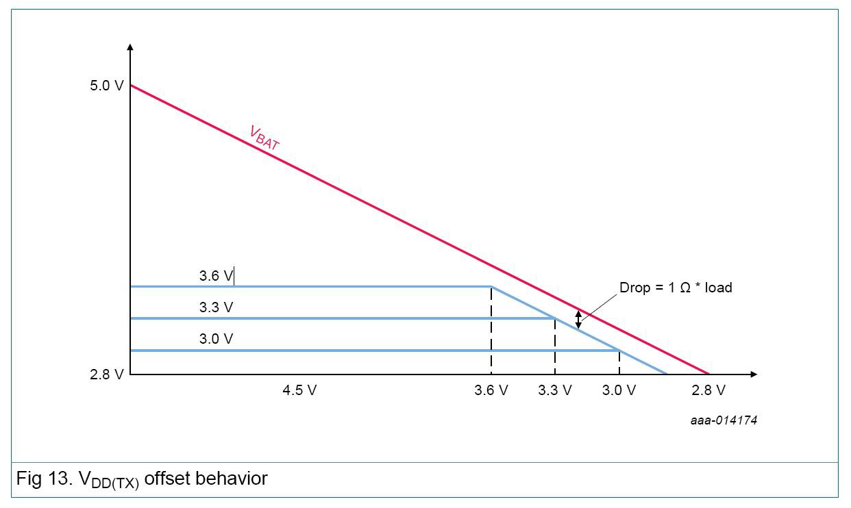
In the “Config 1” scenario an external (Battery) voltage is connected to both the PN7150 VBAT1 and VBAT2 pins.
According to this chart the maximum VDD(TX) can be is 3.6V when VBAT1/VBAT voltage is greater than or equal to 3.6V + TXLDO voltage dropout value.
In the “Config 2” scenario an external (5V) voltage is connected to the PN7150 VBAT1 pin and the VBAT2/VBAT pins is separately powered. Both the OM5578 board and the Mikroe USB Dongle have this configuration.
This options allows for a higher VDD(TX) to be generated.

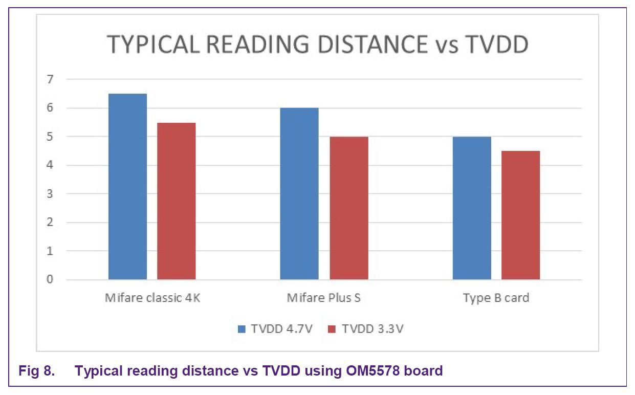
The reason why these configurations matter is that the voltage level on the TX output buffer, which comes from TVDD, can influence the NFC RF reading distance, as depicted here:
As such, the design of the propose PN7150 FeatherWing board will be to allow the user to select what TVDD to use. This can be 5V from the Feather USB pin or 3.7V from a lithium battery (Feather BAT pin) or from the Feather 3V3 pin. This essentially allows the user to setup either "Config 1" or "Config 2", depending on their preference etc.
PN7150 Antenna Interface
The PN7150 is connected to an NFC RF antenna through a matching circuit. So all the components values within the matching circuit are antenna design dependent.
The PN7150 Antenna Design and Matching Guide document (AN11755) recommends a 40 mm x 40 mm antenna, which can be found on the OM5578 interface board and is the spec that will be adopted here too. According to the same document, the PN7150 was designed for Active Load Modulation (ALM), which allows for the use of a smaller antenna.

According to the hardware design document (AN11756), there are three key design rules to apply and then a 4th rule to consider in certain circumstances:
Inductor L0 and Capacitor C0 create a 2nd order low pass (EMC) filter, which is used to reduce the spectrum power amplitude in the high frequency range without altering the meaningful communication signal. The OM5578 schematic shows that L0 is 160nH and C0 is 680pF.
Capacitor's C1 and C2 are used to tune the Poll mode and Listen mode frequency at 13.56MHz and to adapt the equivalent impedance presented on TX1/TX2 at this frequency (70 ohms is recommended). This is referred to as the Matching Circuit. The OM5578 schematic shows that C1 are two capacitors in parallel (56pF and 22pF = 78pF) and C2 is also 2 capacitors in parallel (i.e. 120pF and 2.2pF = 122.2pF). The design document notes that these parallel capacitors are in place as the peak to peak voltage at antenna ends could reach more than 50V depending on the antenna geometrical characteristics. However, if this proves not the case, with final product design, then these can be reduced down to a single capacitor.
Resistor Rq is optionally used to reduce the qualify factor of the antenna when it is above 35 (if it is already below, which is fairly common in embedded equipment environment with ferrite shielding, Rq need not be populated). The OM5578 schematics has Rq = 1.5 Ohms.
Crx and Rrx are for antenna decoupling. The design document notes that if a small antenna is connected to the PN7150, the peak to peak voltage generated at antenna ends will be limited, and this offers the possibility to simplify the RF path circuitry by removing the decoupling Crx caps and connecting directly the Rrx to the antenna ends. The OM5578 schematics has Crx = 1nF and Rrx = 2.2k Ohms.
- High-Q factor (> 20 @ 13.56MHz) is preferred.
- AC Current Characteristics (depending on μ saturation vs. H value)
- Coupling effect (lowest coupling factor vs. distance between coils is preferred)
The following EMC inductors have been verified and properly checked by NXP:
- TDK MLF series (e.g. MLF1608)
- MURATA Multi-layer parts (e.g. LQB18 series) and Wire-wound parts (e.g. LQW18 series)
Then, according to the PN7150 Antenna Design and Matching Guide document (AN11755), the recommendation is for the combination of TX1/RXN and TX2/RXP, but the inverse (TX1/RXP and TX2/RXN) does not have any impact on PN7150 functionality. This rule should make life easier with PCB optimisation.
TO BE CONTINUED...