The basic charging function operates on the stack. Moving charge between between individual batteries is more challenging so I've focused on this area of the design first. To maximize the stack's performance, the balancer must be capable of moving charge to or from any combination of batteries simoultaneously. And, it must be able to monitor the individual battery voltages to assess charge state. All of this requires working around the common mode voltage of the stack.
Here's the conceptual schematic for the balancer section. It depicts a stack of four 12-volt lead-acid batteries but could be extended to taller stacks.
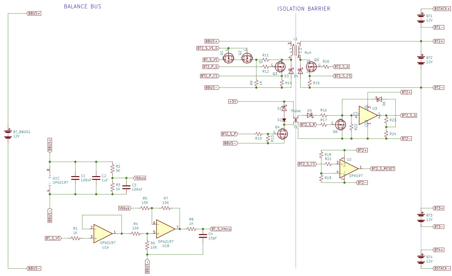
It uses bidirectional isolated flyback transformers operating at 100kHz to transfer charge and to sense battery voltage. The flybacks form an isolation barrier between the stack and what I call the balance bus (BBUS). The BBUS also contains a 12V lead-acid battery (but much smaller than those in the stack, say 9Ah) that powers the controller and serves as a resevoir for charge exchange.
One quarter of the flyback control & sense circuitry is depicted. The secondary is connected to a battery in the stack. The drive circuit is comprised of pulse transformer T1, current sense op-amp U2, and gate driver U3. U2 & U3 function as a Set-Reset latch to maintain a constant on-time of ~ 5uS. The controller's drive pulse of 1uS is transfered across the isolation barrier via T1. U3's gate drive output goes high, Q5 turns on, and L1 begins to charge. Positive feedback to U3's input via D6 maintains the gate drive. As L1 charges the voltage across R15 rises. When it exceeds the voltage set by R18 & R19, U2's output goes high and turns on Q6. The gate drive turns off and the duty cycle terminates. L1 discharges to the battery bus.
The circuitry looks complicated but is really quite simple. It's comprised of a few SOT-123/143 chips and a handful of capacitors & resistors. It operates on the battery's voltage; no regulation is required. Constant on-time is maintained regardless of battery voltage because limits are ratiometric: as the battery voltage varies so does the reference voltage at U2's inverting input. L1's current ramp also changes in proportion to the battery voltage.
I chose this approach because it avoids the need for a microcontroller with firmware, regulated power supplies, and a potentially more sophisticated & expensive communication scheme across the isolation barrier. I also want to be able to centrally control the drive timing for lower EMI: letting the drives operate asynchronously, even at the same frequency, may increase resonant harmonics.
Of course such a simple scheme eliminates direct measurement of battery voltage. The solution is inspired from a Linear Technology application note (AN112) written by Jim Williams & Mark Thoren back in 2007. In it they describe the use of a pulse transformer to measure cell voltages in a stack. A flyback can also be used for this.
To measure the voltage of a battery in the stack, the controller issues a drive pulse to the secondary. During the on time, the voltage imposed on the negative node of L1's primary (Drain of Q3) will be the sum of the voltages of BBUS plus BT2 (minus transformer error and current sense resistor R15 voltage drop). If this voltage can be sampled at the mid-point of the duty cycle then the battery's voltage can be calculated by subtracting BBUS & measurement offset and applying a correction coefficient.
R11 & R9 scale the voltage at Q3's drain and U1A buffers it to eliminate error due to the relatively low impedance created by R4 & R6. U1B is a unity gain differential amplifier that subtracts BBUS from the measurement. U1B's output is sampled by the MCU's ADC, the value is scaled and a correction coefficient applied to derive the battery voltage.
The schematic depicts an analog switch, formed by Q1 & Q2, to select a battery for connection to the differential amplifier. This allows for a single amplifier for the entire stack but at the expense of the additional switches, gate drivers, and control firmware overhead needed for each battery. This scheme also requires n+1 controller pins (1 for the ADC input) versus n ADC inputs if separate differential amps are used for each battery. As I write this I am leaning towards separate amps since they are not expensive and the analog switch is a bit of a kludge. The analog switch might be useful in situations where ample digital controller pins exist but ADC inputs do not.
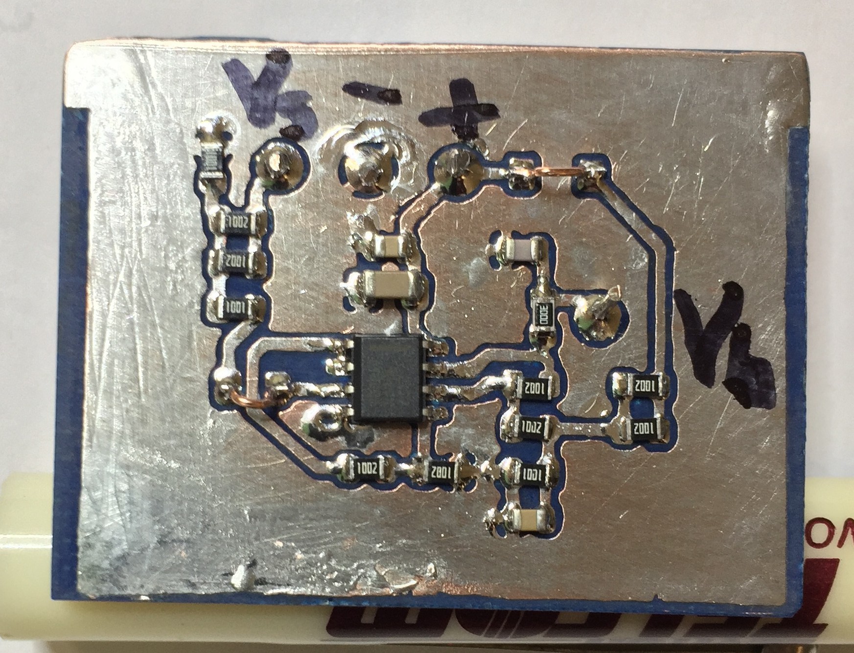
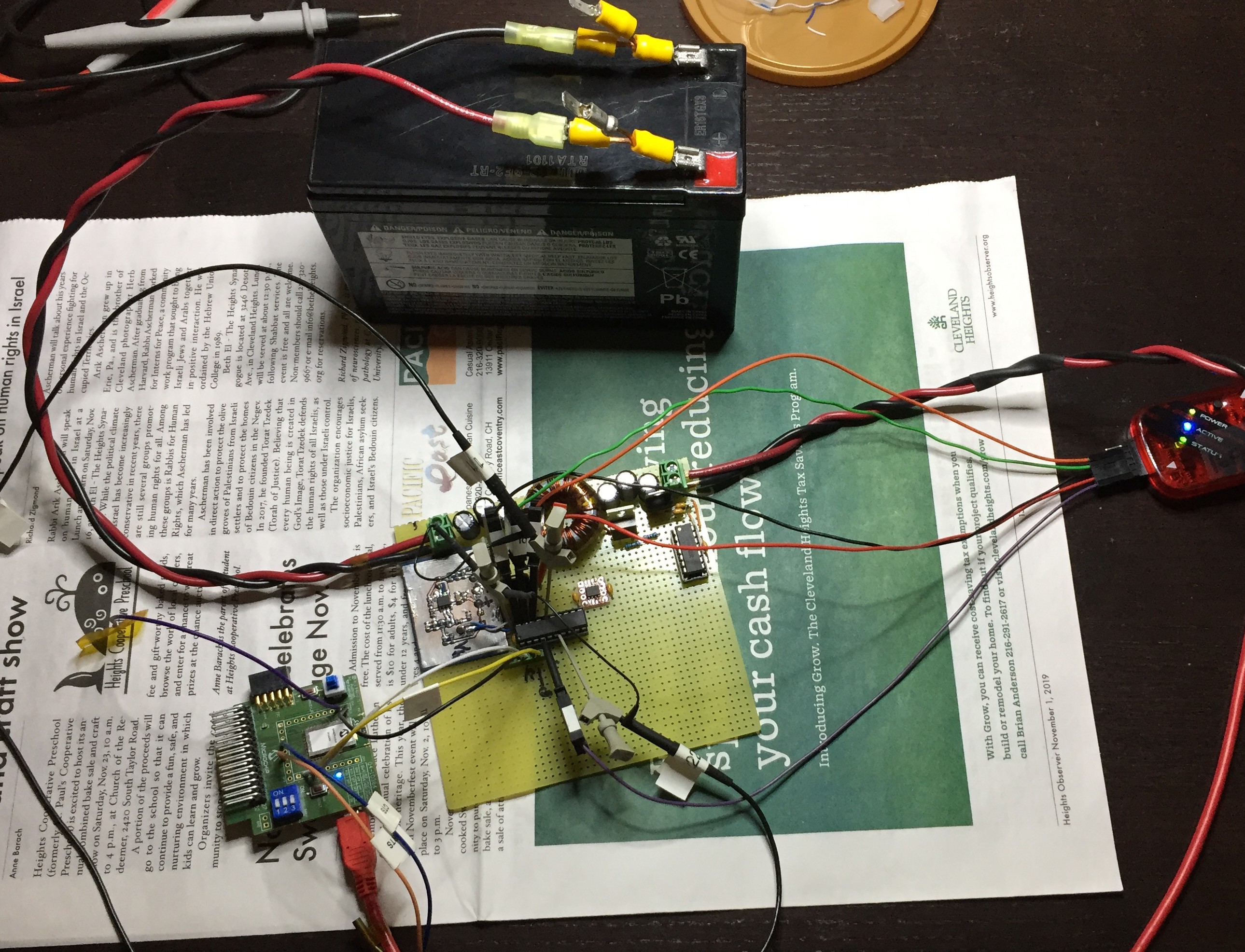
So how well does this actually work? Spice simulations showed that this measurement scheme could achieve +/- 5mV accuracy but I never trust it. I prototyped the flyback with the secondary drive using what I had on hand (digital isolator & conventional gate drive). The primary had only the schottky diode on the negative node. I used a homebrew PCB for the differential amp for better parasitics control and a PIC16F1769 8-bit MCU to generate the drive pulse and perform the acquisition. The secondary was powered by a bench supply to simulate various battery voltages. The primary was powered by a 12V lead-acid 9Ah battery.
Here's the differential amp's output. Channel one is the flyback gate drive and three is the amp output: it's mostly settled by 1.5uS.
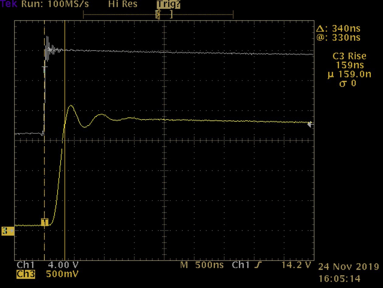
You want to get the measurement as close to the leading edge as possible to minimize the error introduced by the current sense resistor as the inductor's current ramps up (notice the slight downward slope).
A cool feature in some of Microchip's MCUs is the ability to trigger an acquisition using the PWM peripheral's offset feature. The offset trigger can occur anywhere in the PWM period (before, during, or after the duty cycle) and can issue an interrupt or start and ADC conversion. For measuring battery voltage, I've found that a 3uS offset (from start of DC) provides the best accuracy.
With a single sample I've achieved accuracy better than +/- 30mV and, interestingly, with a sample of 10 +/- 50mV. The Excel worksheet provides the supporting data.
One limitation of this method is that it cannot be done during normal operation of the flyback. The obvious is when the primary is moving charge to the battery. But, also when the secondary is moving charge from the battery to BBUS. That's because of the potential for a volt-second imbalance: a battery voltage higher than BBUS won't fully discharge the inductor which will lead to early termination of the duty cycle. Functionally, this isn't a problem and is inherent to the design.
The work-around is to stop charge transfer and run the secondary at 10kHz. This ensures adequate off time for core reset and for the MCU to process the acquired value. Ten samples take 1mS. All of this occurs without interruption to the stack: it continuously supports a load or charge. So in this application it's really not a limitation.
Next step: replace the conventional gate drive in the secondary with the SR latch scheme described here. It's a simple design but I have a habit of missing the obvious.