Being my first SEPIC design, I invested a lot of time reading up on their theory and design. Unlike the more mainstream topologies information is a bit fragmented, so it took a while to assemble what I considered a thorough design model. What I share here is a qualitative discussion that is by no means complete: I found it hard to succinctly describe the component relationships and key design considerations. The supporting mathematical (design) model can be found in the accompanying workbook.
The Limitations of the SEPIC. A machine doesn't need a lot of parts to be complicated, and SMPS demonstrate this well. Worse, a small component count simply means that each one possesses several critical parameters and that changing one cascades thru the entire design. And so it is for the SEPIC: the coupling capacitor and coupled inductor dictate the design.
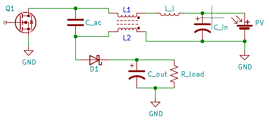
The SEPIC shines for its ability to transparently boost or buck the output voltage while maintaining a constant input current (with a ripple component). It performs best when the input voltage varies about the output by a range dictated by the current and voltage stresses imposed on the circuit elements.
The prototype for this project is spec'd to deliver 250W at 56V with an input of 63V. At 93% efficiency the input current is 4.3A. Skipping the math, the coupled inductor will see over 9A peak since each winding will carry over 4.3A. Add a 20% saturation margin and the inductor's saturation rating must be at least 10.8A. The coupling capacitor's RMS [ripple] current ratting, which is approximately equal to the input current, must be at least 4.3A. These are large values but not unrealistic.
But if this design is expected to deliver 250W with a 10V input, the inductor's saturation current rating would be 47A and the capacitor would require an RMS rating of 28A. Completely untenable.
The variable impedance of a PV system extends the operating regime of the SEPIC into this crazy territory since full power is only attainable at MPP. At 10V with the selected panel about 90W is available, but the supply will only need to deliver 45W (because the final design will interleave two supplies). This keeps the input current relatively constant at ~ 4.9A. Above MPP the current drops rapidly to zero so the design isn't much concerned about operation at higher voltages except tolerating the panel's open circuit voltage under no-load conditions.
The Coupling Capacitor. The coupling capacitor facilitates the unique boost/buck property of the converter. This is because L1 is isolated from the output making duty cycle the sole determinant of output voltage just like the buck/boost topology. But it is also its Achilles heel. Half of the energy delivered to the output flows thru it. This rectangular current waveform creates a high RMS ripple current thru C_ac. Depending on the operating voltages and value selected for C_ac, the ripple voltage adds additional stress. All of this imposes limitations on the type of capacitor that can be used and directly effects cost, size, and reliability.
A small C_ac value requires less board space and generally costs less, but lower values have higher AC ripple and as will be shown later can effect the inductor design and EMI footprint. The polarity across C_ac can also reverse when small values are used, and occurs when the ripple component exceeds the input voltage at maximum load. Non-polarized types are most often used, but polarized variants may be a better choice in higher voltage & ripple current applications.
SEPICs operating at higher voltages and RMS currents limit the type of capacitor that may be used and will likely increase the size & cost of the design. In low voltage designs MLCCs are the obvious choice because of the large capacitance available in small, cheap, low-inductance packages. The problem with MLCCs is their temperature & voltage derating. C0G/NG0 aren't available in voltages much above 50V with values of a few hundred nanofarads. X7Rs are the next best thing but their capacitance drops precipitously as the applied voltage approaches the rated value. Sure, they can be paralleled for higher values & compensation but are still limited to relatively low (<50) operating voltages. Last, their failure mode is a short which connects the input directly to the output.
Film capacitors are a good option for higher voltage designs. They check most boxes: stable temperature & voltage coefficients, low ESR, high operating voltages, wide selection of appropriate values, high reliability, and fail open. The trade-off is size, cost, and some parasitic inductance due to their large package sizes and thru-hole mounting.
Polymer electrolytic capacitors are an alternative in applications where a film cap is being considered. You might be able to get more capacitance in less space for the same or lower cost. They're available with (relatively) low ESR and decent ripple current ratings. Of course, maintaining the polarity across the capacitor by a safe margin becomes important.
Tantalum capacitors can also be used but I stay away from them. They are temperamental and can fail explosively when any of their parameters are exceeded.
The Coupled Inductor. It is possible to consolidate the individual inductors because the windings maintain the same polarity and voltage at all times. The coupled inductor halves the inductance requirement because it must support twice the current. Even though the coupled inductor may be larger, the overall footprint is reduced.
Using a coupled inductor subtly modifies the SEPIC's behavior. The rectangular current thru C_ac resulting from the switching cycle induces an AC ripple voltage across the inductor inversely proportional to C_ac's value. This generates an additional circulating current across both windings of the inductor that distorts the triangular input current ripple waveform, increases EMI, and creates stability problems for the control loop. This problem can be overcome by deliberately introducing leakage inductance to reduce this circulating current.
The Enmeshed Relationship of the Coupled Capacitor & Inductor. The design starts with selecting a value for the coupled inductor, and this is most easily done by establishing a limit on the input ripple current. This limit is usually set as a percent of the input current at maximum load. High input ripple creates more EMI but allows for a smaller inductance and maybe a smaller core. The reverse is also true.
The values for L, L_l, and C_ac are interrelated: a small C_ac value will generate a larger ripple voltage and require a larger leakage inductance to oppose it. L's value influences L_l and C_ac because the smaller the inductor's ripple (e.g. magnetizing) current, the larger the product of L_l & C_ac must be to compensate. This is because C_ac's circulating current must be reduced to a value less than L's input ripple to minimize the distortion.
To summarize, the values for C_ac and L_l are inversely related and the product of C_ac and L_l are directly related to L.
Once a value is chosen for L, the value for C_ac is set. Its value should be as small as possible to minimize cost & space, plus smaller values also offer a wider selection in voltage range and tighter tolerances. But not so small that the required L_l isn't possible (it is not a separate inductor as shown in the schematic).
There are two approaches to establishing the leakage inductance value: by selecting a target input ripple current or setting the circulating current induced by C_ac equal to the magnetizing inductance. The former uses L_l to shift (or steer) input ripple to L2. I have chosen the latter approach since the interleaved design eliminates input ripple as a concern.
Obtaining a specific leakage inductance is dependent on the core type, winding placement, and configuration. With a toroid you can get a lot of leakage inductance by placing each winding on one half of the core. They are my default since they are usually easier to wind, but for this design I'd need a large & expensive core. Instead I went with a gapped RM14. L2 (secondary) is wound first. Leakage inductance is obtained with several layers of insulation (3mil polyimide) wound on top of it and then the winding for L1.
A potential problem with the introduction of L_l is resonance with C_ac. The frequency will likely be well above the control loop's gain and can wreak havoc. An RC dissipative snubber can fix but I haven't decided on this approach yet (but I will probably accommodate on the PCB).
SWITCHING COMPONENTS
In an earlier post I had suggested using a synchronous switch for D1, but after looking at the dissipation and added complexity of a high-side drive it isn't worth it. Q1 and D1 see roughly the same peak currents, and a schottky diode incurs only 1W additional over Q1. So for the prototype I'll keep it simple and stick with a diode.
Discussions
Become a Hackaday.io Member
Create an account to leave a comment. Already have an account? Log In.