I ended my last post with mention of the snubber for C_ac to dampen the resonance with L_l. And, analysis & design of the control loop wasn't done. Completing the design resulted in further modifications and some corrections. An updated design workbook is posted along with a more complete LTspice model. This post addresses five areas:
- Current mode control and slope compensation
- Implementing leakage inductance
- Snubber for C_ac & L_l resonance
- C_ac AC ripple voltage ratings
- Control loop design
Current mode control and slope compensation. Current mode controls peak inductor current; not average and therefore requires slope compensation to prevent subharmonic instabilities. With a PIC MCU the ideal method is to use the Programmable Ramp Generator (PRG) to apply a negative ramp (M) that subtracts from the outer (voltage control) loop error amp signal. This compensated signal is compared to the switch current sense signal to control on-time. The diagram below depicts the peripheral configuration.
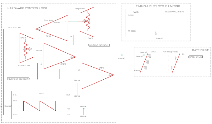
I prefer the use of current transformers whenever possible. They are efficient and require almost no conditioning to provide a clean sense signal. Their major limitations are space and reset time (volts-seconds product).
The value of M is in A/uS but uses the voltage analog of the current sense circuit. So with a sense of 400mv/A and a required M of 0.5A/uS the PRG's ramp would be 200mv/uS. Hence, the design of the sense circuit not only effects the power stage gain but also slope compensation. Other considerations:
- The PRG's minimum ramp is 200mV/uS: the derived M slope must be >=.
- The resolution (e.g. volts per amp) of the current sense circuit: a smaller V/A provides more dynamic range but a lower M value.
- Inductance: a lower L increases the charge/discharge slopes (M1/M2) but can exceed current sense circuit head room.
- CT reset voltage: a function of the volts-seconds product that is effected by the maximum current the CT must measure, on-time, and the V/A value derived from the burden resistor.
- Switching frequency: higher F_s reduces L and increases M at the expense of increased dissipation.
- Input ripple current allowance: setting a higher value reduces L and increaes M but will impact the CT design
- Changes to L or F_s effect the value of C_ac, the induced AC ripple, and L_l requirements of the inductor.
At an F_s of 100kHz I could not achieve an M of 200mV/uS without excessively high input ripple or loss of needed dynamic range in the sense circuit. 200kHz would have been perfect but the switching losses became excessive. 150kHz provided a workable compromise - just barely. So, I plan to include an alternate external positive ramp circuit that allows for smaller than 200mV/uS. For the prototype it can coexist on the PIC without conflict. The downside to this option is additional components and pin consumption. A small ramp can also be problematic due to a smaller S/N ratio that results in jitter in the output.
Implementing leakage inductance. Adding leakage inductance to the coupled inductor is highly dependent on the selected core, bobbin, winding placement, and methods. I have opted for a gapped RM core with a conventional bobbin (e.g. single winding area - not split, etc.) for size and availability from a mainstream supplier. This, along with winding by hand, limits the amount of leakage inductance obtainable: basically how many layers of tape you can place between the windings before running out of window area.
The higher operating frequency allowed for the use of an RM12 (vs. 14 for 100kHz). Testing of several builds showed that ~ 6uH of leakage was the limit (using the outer winding as 'primary' or L1 from the spice schematic). Interestingly, the outer winding always (across different test builds) measured several uH more (inductance) than the inner. I hypothesize this is due to the larger MLT and closer proximity to the core's outer legs which are not gapped.
An alternate way to implement L_l is as a physically separate inductor in front of L1 - which might make sense depending on C_ac sizing requirements. Ultimately I chose to work with the L_l I could obtain from the RM12 and size C_ac accordingly. When considering the snubber for C_ac this worked out quite well since the snubber's dissipation can be significant with small C_ac values (explained in next section).
Here's the numerical analysis of the inductor design. It specifies four strands - two are for each winding of N=18. Note that the winding losses aren't representative due to ripple current steering. The physical build is straightforward:
- L2 wound on bobbin first. Two strands of 22AWG (flat - not twisted) wound in two layers, 9 turns per layer. The layers are wound end-end with no fold-back between layers which makes winding & termination easier since both ends exit at the bottom of the bobbin. One layer of 3mil polyimide tape between each layer.
- Tape layer for L_l, N=25, 3mil polyimide.
- L1 wound on bobbin last. Two strands of 22AWG (flat - not twisted) wound in two layers, 9 turns per layer. The layers are wound end-end with no fold-back between layers. One layer of 3mil polyimide tape between each layer.
Snubber for C_ac & L_l resonance. The revised spice model demonstrates that resonance will occur during startup or a transient (run with & without the snubber). This resonance occurs because C_ac and L_l are coupled throughout the switching cycle. It not only injects EMI into the input supply but can degrade transient response. A snubber is necessary since the resonance is above the control loop's cutoff freqency (F_co).
C_ac & L_l can be treated as an LC filter and critically dampened according to the formula:
1 = R / sqrt(L_l / C_ac) (1)
Where R is the impedance of the damping network, in this case the snubber RC impedance at the resonant frequency. This will lead to a large value for the snubber capacitor, typically 2~4 times C_ac. In my design where C_ac = 3uF, that might require 12uF which is not practical. So I designed the snubber for an under-damped response for what I found to be acceptable in simulation. I expect to make adjustments based on in-circuit validation.
The snubber resistor's dissipation is proportional to the AC ripple voltage across C_ac: small C_ac values with large AC ripple components can induce significant power losses. For example, a C-_ac of 3uF results in a snubber R dissipation of ~ 1W. Halving its value increases dissipation to ~ 3.5W.
C_ac AC ripple voltage ratings. I spent a lot of time fretting over the maximum AC RMS voltage graphs when selecting C_ac (Metallized Polyester Film caps) and this imposed an additional constraint on the design. Calculated / simulation RMS currents were always well within limits. But, AC RMS voltage values were often out of spec or close. To ensure I had some margin I paralleled two and will evaluate the temperature rise in circuit. As a consolation I am able to use the same cap for both C_ac and the snubber.
Control loop design. An advantage of a coupled inductor SEPIC is that the power stage small signal model has a single pole response below the resonant frequency of C_ac & L_l. Further, since a snubber is implemented to dampen that resonance, the buck/boost transfer function can be used to plot gain & phase shift:
A = Ri / (Vramp_max – T_on * M) * [I_T - j * V_out / X_L1] (2)
Where:
A = circuit gain @ f,
Ri = Volts/Amp of current sense circuit,
Vramp_max = ramp voltage at start of switching period (e.g. max. output of voltage
EA),
T_on = switch on-time @ MPP,
M = compensation slope, V/uS,
I_T = I_in + I_out
The single pole gives a 90 degree phase shift. There is also a zero whose location varies based on load. For use in a PV design the lowest frequency is at MPP. The zero must be accounted for to ensure that there is adequate gain margin.
Because there is only a single pole & zero a type two error amp is used. A cross-over frequency, Fco, is selected along with frequencies for the EA zero & pole to allow suitable margin for Fco to occur with a -1 slope.
Wrap-up. The design workbook covers everything that's been discussed and shows how changing one parameter effects the rest of the design.
The LTspice model is representative of the intended power stage and was used to validate (sometimes with approximations) the design workbook. The control loop was not included and the behavioral logic components (U1, A1, A2) are used to emulate peak current limiting only (not current mode control). This was necessary to obtain the expected C_ac & L_l resonance behavior. Inductor L3 represents the leakage inductance of the coupled inductor (L1, L2).
Discussions
Become a Hackaday.io Member
Create an account to leave a comment. Already have an account? Log In.