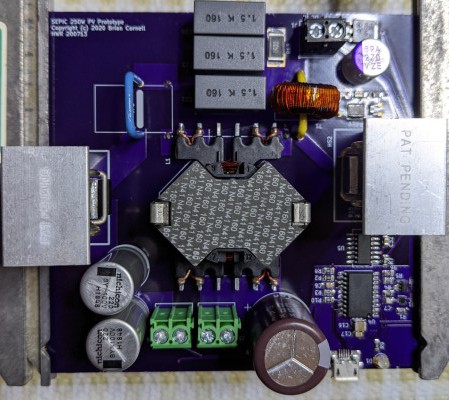
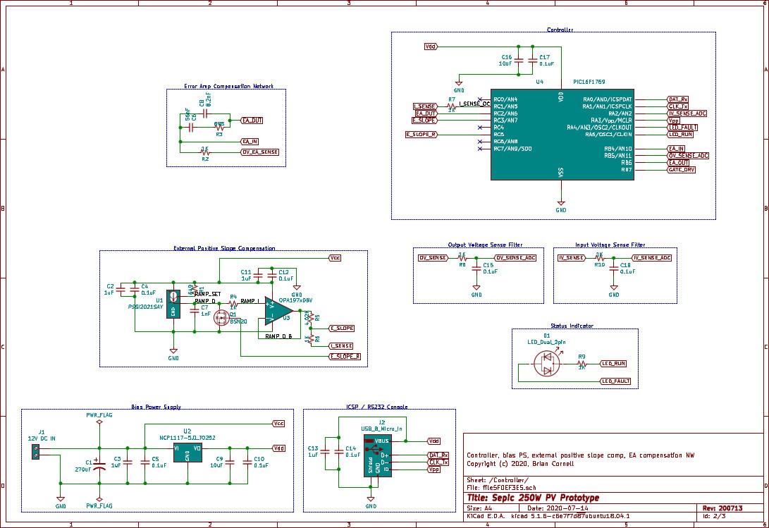
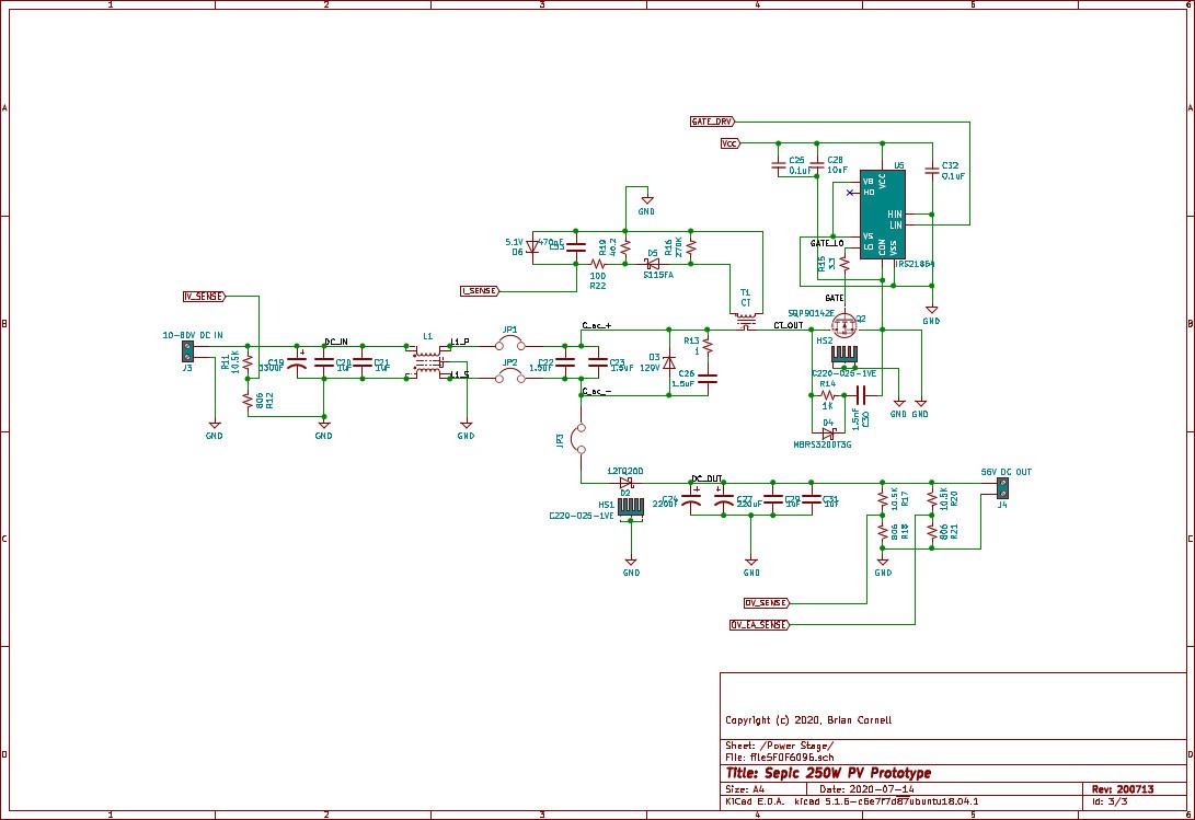
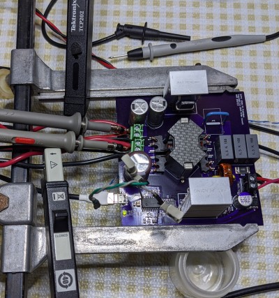
Okay, I finally got this thing built and completed a preliminary evaluation. The Kicad, MPLAB projects, and updated design workbook are posted in the files section but don't rush to build it.
Specs:
- Input voltage: 10 - 80 volts
- Input current: nominal 4.3A @ 62V, full power
- Output voltage: 56V
- Output current: 4.5A (max)
- Maximum continuous power @ V_in > 60V: 250W
- Maximum continuous power @ V_in 10V: 45W
- Control mode: average current
- Bias supply: 12V
- Operating temperature: -20 - +50C (not validated)
- Design efficiency: 93%
Note that the power derates as the input voltage declines. This keeps the input current relatively constant and tracks with the maximum power available from the PV panels. Initial efficiency was closer to 90% but after improvements to the output diode, D2, it achieved 92% efficiency at 250W.
Overall, it worked as designed. The control loop is stable thru all operating regimes (with both external & internal ramps) and the coupled inductor / ripple current steering is solid. The coupling capacitor, C_ac, and associated snubber performed as expected with no resonance and within expected operating limits.
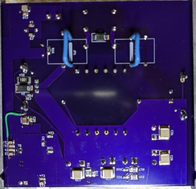
It does have some problems that are mostly the result of inattention because of my hyper-focus on SEPIC specific aspects of the design. The layout is also sub-optimal with several 'loop' jumpers to accommodate current probes at the expense of increased inductive parasitics.
Switch snubber. The most serious is switch Q2 and its snubber. The root problem is the ring at turn-off. CH1=D-S volts, CH2=current sense (CT) circuit output, CH3=L1 primary current, CH4=L1 'secondary' (coupled) current.
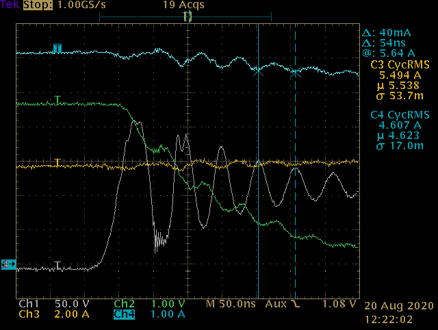
The snubber does not fully dampen it but is still absorbing 3+W more than anticpated (for total ~ 4.5W). That, combined with inadequate Cu area on the PCB, sends the snubber resistor north of 200C in 30 seconds at full power. Since a proper fix would be difficult, and this wasn't the focus of the build, I decided not to fix and worked around (limited high-power run-times, forced-air cooling) during the evaluation.
Amazingly, Q2 did not avalanche/fail and ran close to predicted temperature. In an attempt to measure the non-dampened ring, I did remove the snubber but that resulted in the switch's immediate failure. The revised design will use a non-dissipative snubber that will probably send the recovered energy to the bias supply. To ensure robustness the revised design will use a different MOSFET with a higher D-S rating.
Output diode. The output diode, D2, had similar problems at the anode during turn-off because I hadn't included a snubber for it. CH1=voltage at anode referenced to ground, CH3=voltage at cathode referenced to ground, CH4=diode current, M1=CH3+CH1 (incorrect).
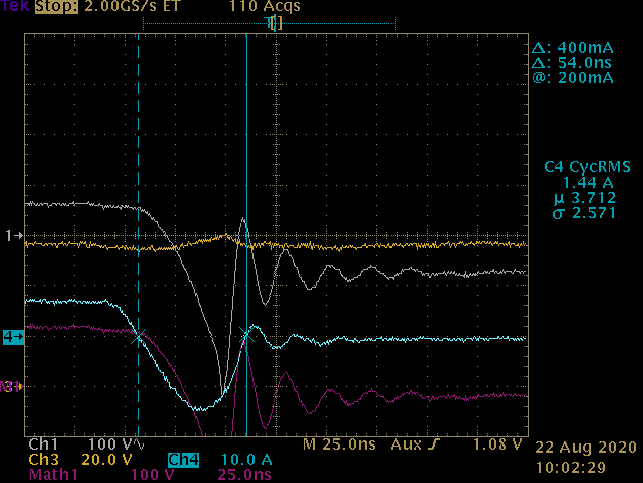
Its reverse voltage rating (200V) was being exceeded and it was avalanching - resulting in ~ 5W of additional losses (incredibly, albeit a Schottky, it did't fail). I fashioned an RC snubber which eliminated the ring except for the initial negative inductive swing but the high losses continued. I replaced the schottky with a 400V fast recovery diode (but higher forward voltage) and netted 4W. Interestingly, there is still a 10A excursion during recovery. M1 correctly shows the voltage across the diode and it is well within its V_r (CH3-CH1).
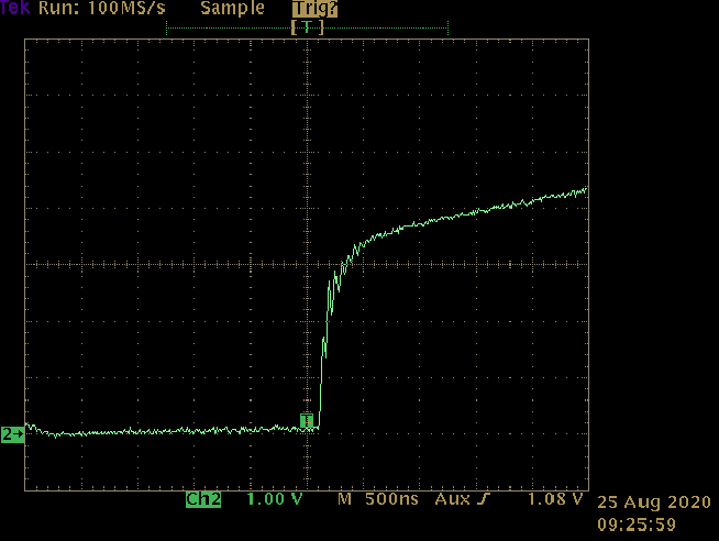
External slope. The external slope compensation circuit worked well but I made the mistake of powering it with Vdd (+5V) instead of Vcc (+12V). The problem with a 5V supply is that the slope becomes asymptotic above ~ 4.5V. Hacking the PCB to reconnect to Vcc and adjusting R1 for a ~ 1V/uS fixed the problem.
The external slope does have a ~ 500nS non-linear region at the start of the duty cycle due to propagation delays in the constant current source but this did not induce control problems at no/light-load conditions.
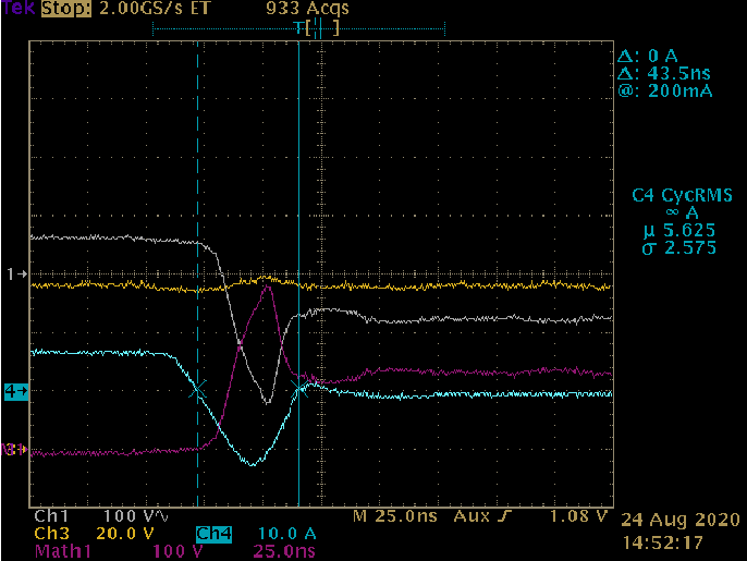
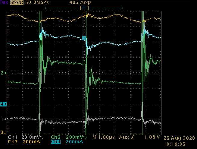
Current sense switching spikes. During initial evaluation the over-current protection would engage when loading at 250W with input voltages < 60V. A review of the current transformer circuit's output showed what I thought were noise spikes. These are uncharacteristic for a CT and I already had a low-pass filter on the output - which should have been my first hint.
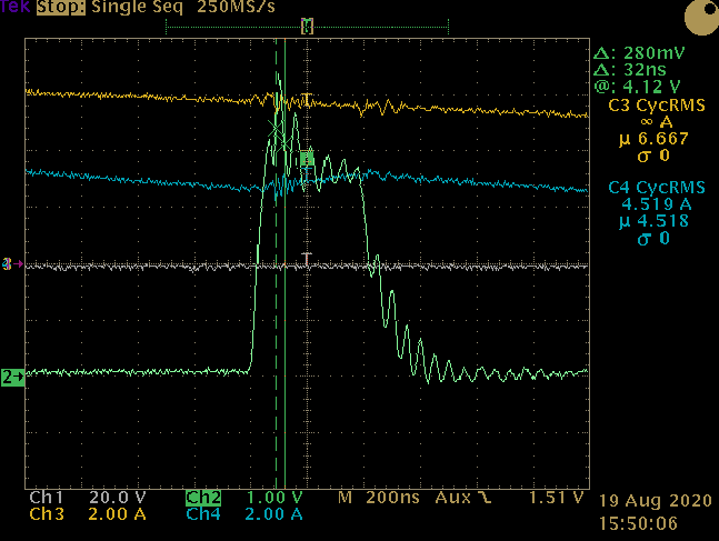
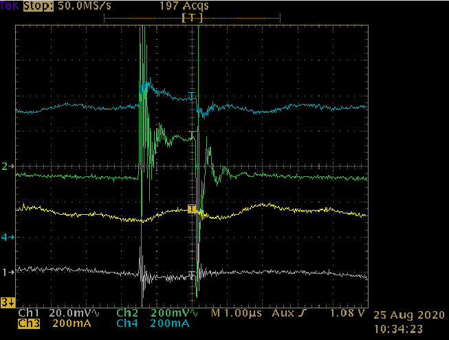
I increased the value of C33 which, as it turns out, treated the symptom but not the problem. The locus was D2's reverse recovery current, so the CT was right! Channel two shows the 'corrected' leading edge of the sense signal.
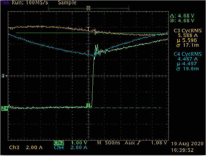
Still a bit of noise but not enough to cause problems. Same setup / trace after fixing D2:
All leading edge noise is gone; I should probably revert the low-pass filter cap, C33. The lesson here is to fully characterize before diving in to address specifc problems.
Control loop stability. I did not perform formal transient testing for a few reasons. First, the intended application, a battery charger, does not demand fast response. Second, the other testing done to the unit provided ample opportunity to observe instability: hot, excessive loading, start/stop at full loads, etc. Third, this specific design isn't going anywhere: its purpose is to qualify the SEPIC for the intended application and my design approach. That said, I did perform no->full load tests using an electronic load (HP 6063B) in constant current & resistance modes. The goal was to baseline the response and make sure that no gremlins were lurking.
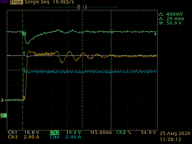
The test regiment applied a constant full load to the unit while running with no load. The load is turned on & left on; not a pulse. Full load is defined as the maximum power the unit will deliver at the regulated output voltage for a given input voltage while running hot. An HP 6030A powered the unit with its current limit set to 9A to emulate the maximum current available from the PV array. Testing was performed in 10V increments from 10-60 volts using both the external and internal slope compensation ramps.
Channel setup: 1=V_in, 2=V_out, 3=I_in, 4=I_out. Channel 2 triggers on a declining output voltage. Passive 1x probes with soldered tip grounds were connected directly to the in/output terminals. Tek TCP202 current probes clamped to power leads as close to terminals as possible.
These traces are for 40V/3.8A and 10V/800mA respectively using the external ramp:
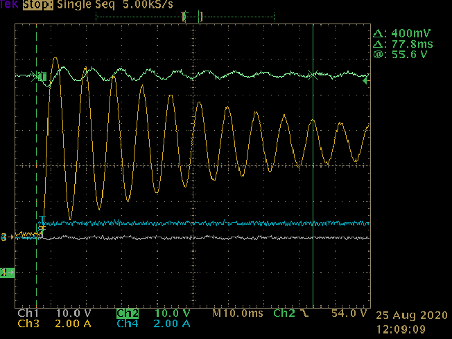
These are for 40V/3.6A and 10V/800mA using the internal ramp:
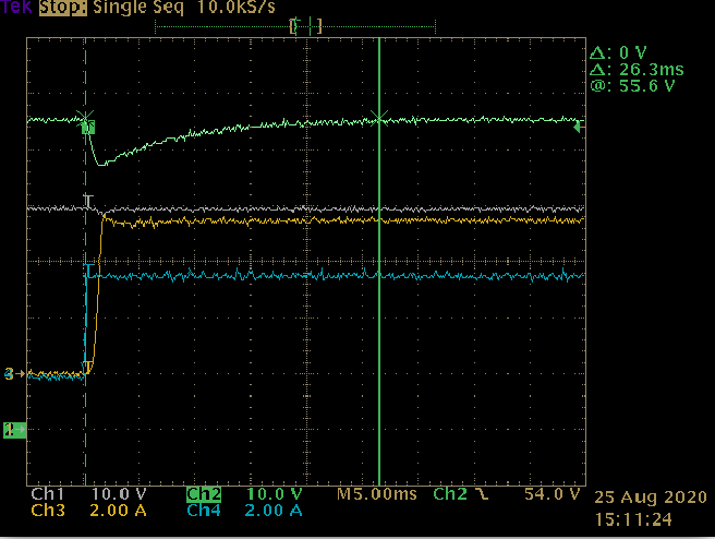
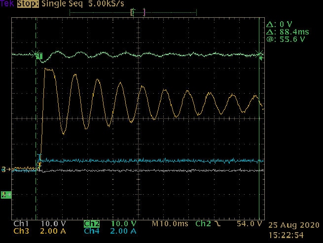
Looks like the external ramp's slope value (probably the compensation network too) could use some fine tuning. Predictably, the internal ramp's slope is a bit over-damped but eliminates all resonance except at 10V. The trade-off is that this eliminates some headroom that the external slope has to obtain higher power at lower input voltages. In spite of this the internal ramp delivers rated power across the operating spectrum for the application.
In/output voltage & current ripple. A key design parameter for this project is to minimize input current ripple because of the long lead lengths associated with PV installations. While the interleaved configuration of two SEPICs operating at 180 degrees with respect to each other should address this it was important to validate that ripple current steering worked as designed.
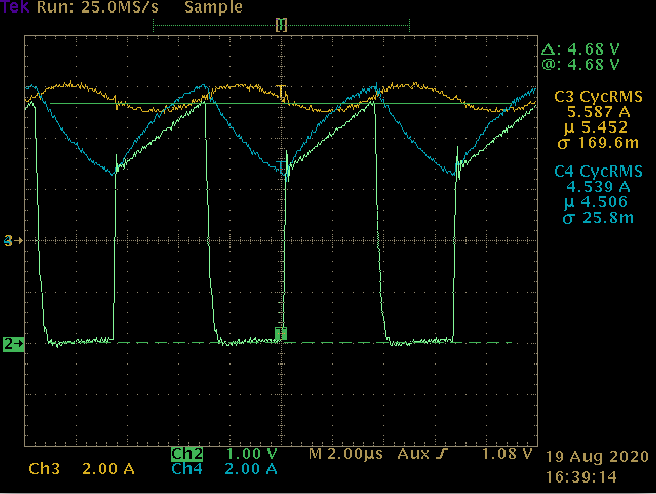
The channel setup is the same as for the control loop but the current channels are scaled to show the AC component. The TCP202 current probes & TDS784C don't allow AC coupling so the offset feature is used. This trace is for V_in=50V, I_in ~ 5.5A, and P_out=250W.
And this one is for V_in=20V, I_in > 7A, and P_OUT=125W.
In both cases input current ripple is less than 200mA RMS and voltage ripple less than 20mV. There is considerable switching noise on the output which is typical for a flyback topology including the SEPIC. Even with this the ripple current on the output is less than 200mA RMS.
Another way to view this is to examine the current wave forms of the coupled inductor.
This trace was taken while working on the CT problem. V_in=50V, P_out=250W. CH3=L1 primary, CH4=L1 coupled. While the primary winding's RMS current is higher it is a sinusoidal waveform with a smaller amplitude. Clearly, most of the ripple current has been shifted to the coupled winding which shows a significant AC component.
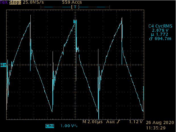
C_ac Ripple Voltage. I had a lot of concern that the ripple voltage across C_ac would exceed the manufacturer's spec and cause heating problems in the caps. Turns out the model was correct and the worst case ripple was as predicted. The trace below was taken with a Tek P5200 differential probe with V_in=62V, P_OUT=250W.
Coupled inductor. The as-built version matches the build spec in the previous log but does include an additional 1/2-turn on each winding since it terminates to opposite sides. This bumped up the primary inductance a bit but didn't materially effect performance.
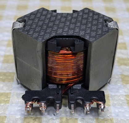
Pin assignments:
- 11/12 - primary (+) in
- 1/2 - primary (-) out
- 7/8 - coupled (+) in
- 5/6 - coupled (-) out
Primary winding measured values:
- L=60.431uH
- L_l=5.6uH
- F_r=1.510MHz
- C_p=183pF
Secondary winding measured values:
- L=54.575uH
- L_l=5.139uH
- F_r=1.558MHz
- C_p=191pF
F_r is the resonant frequency and C_p is the calculated parasitic capacitance using F_r and L:
1 / ((2 * pi * F_r)^2 * L) (1)
Building it. I never intended to use this design for anything but validating the basics of the SEPIC and learning, so I wouldn't recommend building without the modifications discussed here. Even then there are thermal management issues, it lacks a proper bias supply & other circuit protection elements. The control firmware is a stripped-down refinement of my MPPTPROTO project that, like the hardware, contains no failure mode or protection limits.
That said, it's a great starting point for a refined design. Be sure to follow proper safety practices since you'll be exposed to high voltages, currents, and temperatures.
Next steps. I'm going to prototype the 500W interleaved design and incorporate the improvements identified here. Part of this will be to confirm the controller that will be used in the final design (likely a PIC16F1776), gate driver, and whether it is worth exchanging the output diode for a synchronous drive. I really like the simplicity of a single low-side switch, and with the revisions made to this prototype the losses are acceptable.
Prototyping the full interleave setup will also allow me to properly evaluate thermal management and how this thing will be assembled (e.g. enclosure & environmentals): those are critical to decisions on layout, which impact thermal management, footprint, EMI, component selection, efficiency - pretty much everything.
Last but not least, the SEPIC is a fourth-order converter and I need to study the effects of interleaving two of them on the control loop & other stability issues. A single, outer, voltage control loop will connect to each converter's inner current control loop so, component tolerances & layout aside, output power should be balanced. But this too must be verified.
Parallel to this I'll start to flush-out the charge balancer and how it integrates with the charger section. Prototyping for the full stack will help drive most of the key decisions and help eliminate surprises.
Conceptually, I see the charger & balancer functioning somewhat independently with an I2C or SPI connection between them. The charger's controller would function as the master to collect data from the balancer (status, health, etc.) and to control when balancing can be done.
Discussions
Become a Hackaday.io Member
Create an account to leave a comment. Already have an account? Log In.